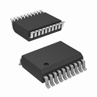
ISL22444TFV20Z Intersil, ISL22444TFV20Z Datasheet - Page 12

ISL22444TFV20Z
Manufacturer Part Number
ISL22444TFV20Z
Description
IC POT DGTL 256TP LN LP 20-TSSOP
Manufacturer
Intersil
Series
XDCP™r
Datasheet
1.ISL22444WFV20Z.pdf
(19 pages)
Specifications of ISL22444TFV20Z
Taps
256
Resistance (ohms)
100K
Number Of Circuits
4
Temperature Coefficient
45 ppm/°C Typical
Memory Type
Non-Volatile
Interface
SPI, 3-Wire Serial
Voltage - Supply
2.25 V ~ 5.5 V
Operating Temperature
-40°C ~ 125°C
Mounting Type
Surface Mount
Package / Case
20-TSSOP
Resistance In Ohms
100K
Lead Free Status / RoHS Status
Lead free / RoHS Compliant
contains all zeroes (WRi[7:0]= 00h), its wiper terminal (RWi)
is closest to its “Low” terminal (RLi). When the WRi register
of a DCP contains all ones (WRi[7:0]= FFh), its wiper
terminal (RWi) is closest to its “High” terminal (RHi). As the
value of the WRi increases from all zeroes (0) to all ones
(255 decimal), the wiper moves monotonically from the
position closest to RLi to the closest to RHi. At the same
time, the resistance between RWi and RLi increases
monotonically, while the resistance between RHi and RWi
decreases monotonically.
While the ISL22444 is being powered up, the WRi is reset to
80h (128 decimal), which locates RWi roughly at the center
between RLi and RHi. After the power supply voltage
becomes large enough for reliable non-volatile memory
reading, the WRi will be reloaded with the value stored in a
non-volatile Initial Value Register (IVRi). All the IVRs are
factory programmed with 80h.
The WRi and IVRi can be read or written to directly using the
SPI serial interface as described in the following sections.
Memory Description
The ISL22444 contains four non-volatile 8-bit Initial Value
Registers (IVRi), eleven non-volatile 8-bit General Purpose
(GP) registers, four volatile 8-bit Wiper Registers (WRi), and
volatile 8-bit Access Control Register (ACR). The memory
map of ISL22444 is in Table 1.
ADDRESS
(hex)
10
E
D
C
B
A
F
9
8
7
6
5
4
3
2
1
0
General Purpose
General Purpose
General Purpose
General Purpose
General Purpose
General Purpose
General Purpose
General Purpose
General Purpose
General Purpose
General Purpose
NON-VOLATILE
TABLE 1. MEMORY MAP
IVR3
IVR2
IVR1
IVR0
N/A
12
Reserved
VOLATILE
WR3
WR2
WR1
WR0
ACR
N/A
N/A
N/A
N/A
N/A
N/A
N/A
N/A
N/A
N/A
N/A
ISL22444
The non-volatile registers (IVRi) at address 0, 1, 2 and 3
contain initial wiper position and volatile registers (WRi)
contain current wiper position.
The register at address 0Fh is a read-only reserved register.
Information read from this register should be ignored.
The non-volatile IVRi and volatile WRi registers are
accessible with the same address.
The Access Control Register (ACR) contains information
and control bits described below in Table 2.
The VOL bit (ACR[7]) determines whether the access to
wiper registers WRi or initial value registers IVRi.
If VOL bit is 0, the non-volatile IVRi and General Purpose
registers are accessible. If VOL bit is 1, only the volatile WRi
are accessible. Note: value that is written to IVRi register
also is written to the corresponding WRi. The default value of
this bit is 0.
The SHDN bit (ACR[6]) disables or enables Shutdown
mode. When this bit is 0, DCP is in Shutdown mode, i.e.
each DCP is forced to end-to-end open circuit and RWi is
shorted to RLi as shown on Figure 15. Default value of
SHDN bit is 1.
Setting SHDN bit to 1 is returned wipers to prior to Shutdown
Mode position.
The WIP bit (ACR[5]) is a read-only bit. It indicates that non-
volatile write operation is in progress. The WIP bit can be
read repeatedly after a non-volatile write to determine if the
write has been completed. It is impossible to write or read to
the WRi or ACR while WIP bit is 1.
The SDO bit (ACR[1]) configures type of SDO output pin.
The default value of SDO bit is 0 for Push - Pull output. SDO
pin can be configured as Open Drain output for some
application. In this case, an external pull up resistor is
required. See “Applications Information” on page 14.
SPI Serial Interface
The ISL22444 supports an SPI serial protocol, mode 0. The
device is accessed via the SDI input and SDO output with
data clocked in on the rising edge of SCK, and clocked out
NAME
BIT #
BIT
FIGURE 15. DCP CONNECTION IN SHUTDOWN MODE
TABLE 2. ACCESS CONTROL REGISTER (ACR)
VOL SHDN WIP
7
6
5
4
0
RHi
RWi
RLi
3
0
2
0
SDO
1
May 24, 2007
FN6426.0
0
0


