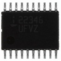
ISL22346UFV20Z Intersil, ISL22346UFV20Z Datasheet - Page 11

ISL22346UFV20Z
Manufacturer Part Number
ISL22346UFV20Z
Description
IC POT DGTL 128TP LN LP 20-TSSOP
Manufacturer
Intersil
Series
XDCP™r
Specifications of ISL22346UFV20Z
Taps
128
Resistance (ohms)
50K
Number Of Circuits
4
Temperature Coefficient
80 ppm/°C Typical
Memory Type
Non-Volatile
Interface
I²C, 2-Wire Serial
Voltage - Supply
2.7 V ~ 5.5 V
Operating Temperature
-40°C ~ 125°C
Mounting Type
Surface Mount
Package / Case
20-TSSOP
Resistance In Ohms
50K
End To End Resistance
50kohm
Resistance Tolerance
± 20%
No. Of Steps
128
Supply Voltage Range
2.7V To 5.5V
Control Interface
I2C
No. Of Pots
Quad
Rohs Compliant
Yes
Lead Free Status / RoHS Status
Lead free / RoHS Compliant
Available stocks
Company
Part Number
Manufacturer
Quantity
Price
Company:
Part Number:
ISL22346UFV20Z
Manufacturer:
Intersil
Quantity:
652
Company:
Part Number:
ISL22346UFV20Z-TK
Manufacturer:
Intersil
Quantity:
950
Pin Descriptions
Potentiometers Pins
RHI AND RLI (i = 0, 1, 2 OR 3)
The high (RHi) and low (RLi) terminals of the ISL22346 are
equivalent to the fixed terminals of a mechanical
potentiometer. RHi and RLi are referenced to the relative
position of the wiper and not the voltage potential on the
terminals. With WRi set to 127 decimal, the wiper will be
closest to RHi, and with the WRi set to 0, the wiper is closest
to RLi.
RWI (i = 0, 1, 2 OR 3)
RWi is the wiper terminal and is equivalent to the movable
terminal of a mechanical potentiometer. The position of the
wiper within the array is determined by the WRi register.
SHDN
The SHDN pin forces the resistor to end-to-end open circuit
condition on RHi and shorts RWi to RLi. When SHDN is
returned to logic high, the previous latch settings put RWi at
the same resistance setting prior to shutdown. This pin is
logically ANDed with SHDN bit in ACR register. I
is still available in shutdown mode and all registers are
accessible. This pin must remain HIGH for normal operation.
Bus Interface Pins
SERIAL DATA INPUT/OUTPUT (SDA)
The SDA is a bidirectional serial data input/output pin for I
interface. It receives device address, operation code, wiper
address and data from an I
rising edge of the serial clock SCL, and it shifts out data after
each falling edge of the serial clock.
SDA requires an external pull-up resistor, since it is an open
drain input/output.
SERIAL CLOCK (SCL)
This is the serial clock input of the I
requires an external pull-up resistor, since it is an open drain
input.
DEVICE ADDRESS (A2 - A0)
The address inputs are used to set the least significant 3 bits
of the 7-bit I
address serial data stream must match with the Address
FIGURE 15. DCP CONNECTION IN SHUTDOWN MODE
2
C interface slave address. A match in the slave
2
C external master device at the
11
RH
RW
RL
2
C serial interface. SCL
2
C interface
2
C
ISL22346
input pins in order to initiate communication with the
ISL22346. A maximum of 8 ISL22346 devices may occupy
the I
Principles of Operation
The ISL22346 is an integrated circuit incorporating four
DCPs with their associated registers, non-volatile memory
and an I
between a host and the potentiometers and memory. The
resistor arrays are comprised of individual resistors
connected in series. At either end of the array and between
each resistor is an electronic switch that transfers the
potential at that point to the wiper.
The electronic switches on the device operate in a “make
before break” mode when the wiper changes tap positions.
When the device is powered down, the last value stored in
IVRi will be maintained in the non-volatile memory. When
power is restored, the contents of the IVRi are recalled and
loaded into the corresponding WRi to set the wipers to the
initial value.
DCP Description
Each DCP is implemented with a combination of resistor
elements and CMOS switches. The physical ends of each
DCP are equivalent to the fixed terminals of a mechanical
potentiometer (RH and RL pins). The RW pin of each DCP is
connected to intermediate nodes, and is equivalent to the
wiper terminal of a mechanical potentiometer. The position
of the wiper terminal within the DCP is controlled by volatile
Wiper Register (WR). Each DCP has its own WR. When the
WR of a DCP contains all zeroes (WR[6:0]= 00h), its wiper
terminal (RW) is closest to its “Low” terminal (RL). When the
WR register of a DCP contains all ones (WR[6:0]= 7Fh), its
wiper terminal (RW) is closest to its “High” terminal (RH). As
the value of the WR increases from all zeroes (0) to all ones
(127 decimal), the wiper moves monotonically from the
position closest to RL to the closest to RH. At the same time,
the resistance between RW and RL increases monotonically,
while the resistance between RH and RW decreases
monotonically.
While the ISL22346 is being powered up, all four WRs are
reset to 40h (64 decimal), which locates RW roughly at the
center between RL and RH. After the power supply voltage
becomes large enough for reliable non-volatile memory
reading, all WRs will be reload with the value stored in
corresponding non-volatile Initial Value Registers (IVRs).
The WRs can be read or written to directly using the I
serial interface as described in the following sections. The
I
03h to access the WR of DCP0, DCP1, DCP2 or DCP3
respectively.
2
C interface Address Byte has to be set to 00h, 01h, 02h or
2
C serial bus.
2
C serial interface providing direct communication
September 3, 2009
2
FN6177.2
C


