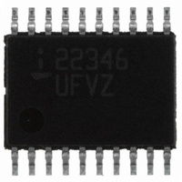
ISL22346UFV20Z Intersil, ISL22346UFV20Z Datasheet

ISL22346UFV20Z
Specifications of ISL22346UFV20Z
Available stocks
Related parts for ISL22346UFV20Z
ISL22346UFV20Z Summary of contents
Page 1
... A1 A0 RH1 RL1 RW1 CAUTION: These devices are sensitive to electrostatic discharge; follow proper IC Handling Procedures. | 1-888-INTERSIL or 1-888-468-3774 Intersil (and design) and XDCP are registered trademarks of Intersil Americas Inc. All other trademarks mentioned are the property of their respective owners. ISL22346 FN6177 ° ...
Page 2
... Ordering Information PART NUMBER PART (Note) MARKING ISL22346UFV20Z* 22346 UFVZ ISL22346UFRT20Z* 223 46UFZ ISL22346WFV20Z* 22346 WFVZ ISL22346WFRT20Z* 223 46WFZ *Add “-TK” suffix for tape and reel. Please refer to TB347 for details on reel specifications. NOTE: These Intersil Pb-free plastic packaged products employ special Pb-free material sets, molding compounds/die attach materials, and 100% matte tin plate plus anneal (e3 termination finish, which is RoHS compliant and compatible with both SnPb and Pb-free soldering operations) ...
Page 3
... EPAD* *Note: PCB thermal land for QFN EPAD should be connected to GND plane or left floating. For more information refer to http://www.intersil.com/data/tb/TB389.pdf 3 ISL22346 PIN NAME A1 Device address input for the I VCC Power supply pin SHDN Shutdown active low input RH0 “High” terminal of DCP0 RL0 “ ...
Page 4
... Thermal Resistance (Typical) 20 Lead TSSOP (Note 0 Lead TQFN (Notes Maximum Junction Temperature (Plastic Package +150°C Pb-free Reflow Profile . . . . . . . . . . . . . . . . . . . . . . . . .see link below CC http://www.intersil.com/pbfree/Pb-FreeReflow.asp Recommended Operating Conditions Temperature Range (Extended Industrial .-40°C to +125° 2.7V to 5.5V CC Power Rating . . . . . . . . . . . . . . . . . . . . . . . . . . . . . . . . . . . . . .15mW Wiper Current . . . . . . . . . . . . . . . . . . . . . . . . . . . . . . . . . . . . ±3.0mA ...
Page 5
Analog Specifications Over recommended operating conditions, unless otherwise stated. (Continued) SYMBOL PARAMETER TC Ratiometric Temperature Coefficient V (Note 12) RESISTOR MODE (Measurements between R RINL Integral Non-linearity (Note 16) RDNL Differential Non-linearity (Note 15) Roffset Offset (Note 14) R DCP ...
Page 6
Operating Specifications Over the recommended operating conditions, unless otherwise specified. (Continued) SYMBOL PARAMETER V Ramp V Ramp Rate Power-up Delay D EEPROM SPECIFICATION EEPROM Endurance EEPROM Retention t Non-volatile Write Cycle Time WC (Note 19) SERIAL INTERFACE ...
Page 7
Operating Specifications Over the recommended operating conditions, unless otherwise specified. (Continued) SYMBOL PARAMETER t SDA and SCL Fall Time F Cb Capacitive Loading of SDA or SCL Rpu SDA and SCL Bus Pull-up Resistor Off-chip t A2, A1 and A0 ...
Page 8
SDA vs SCL Timing SCL t SU:STA t HD:STA SDA (INPUT TIMING) SDA (OUTPUT TIMING) A0, A1, and A2 Pin Timing START SCL SDA A0, A1 Typical Performance Curves 100 V = 3.3V +125° ...
Page 9
Typical Performance Curves 0 2.7V CC 0 5. TAP POSITION (DECIMAL) FIGURE 3. DNL vs TAP POSITION IN VOLTAGE DIVIDER MODE FOR 10kΩ (W) 1.3 10k 1.1 0.9 ...
Page 10
Typical Performance Curves 1.0 0 2. 5.5V CC 10k -0.5 -1.0 -40 - TEMPERATURE (ºC) FIGURE 9. END TO END R % CHANGE vs TOTAL TEMPERATURE 300 250 200 150 50k ...
Page 11
Pin Descriptions Potentiometers Pins RHI AND RLI ( The high (RHi) and low (RLi) terminals of the ISL22346 are equivalent to the fixed terminals of a mechanical potentiometer. RHi and RLi are referenced to ...
Page 12
Memory Description The ISL22346 contains seven non-volatile and five volatile 8-bit registers. The memory map of ISL22346 is on Table 1. The four non-volatile registers (IVRi) at address and 3 contain initial wiper value and volatile registers ...
Page 13
TABLE 4. IDENTIFICATION BYTE FORMAT Logic values at pins A2, A1, and A0 respectively (MSB) SCL SDA START FIGURE 16. VALID DATA CHANGES, START AND STOP CONDITIONS SCL FROM MASTER SDA OUTPUT FROM TRANSMITTER SDA ...
Page 14
S SIGNALS T FROM THE A IDENTIFICATION MASTER R BYTE WITH T R SIGNAL AT SDA SIGNALS FROM THE SLAVE Write Operation A Write operation requires a START condition, followed ...
Page 15
... Dimensions D2 and E2 are for the exposed pads which provide improved electrical and thermal performance. 8. Nominal dimensions are provided to assist with PCB Land Pattern Design efforts, see Intersil Technical Brief TB389. 9. Features and dimensions A2, A3, D1, E1, P & θ are present when Anvil singulation method is used and not present for saw singulation ...
Page 16
... Accordingly, the reader is cautioned to verify that data sheets are current before placing orders. Information furnished by Intersil is believed to be accurate and reliable. However, no responsibility is assumed by Intersil or its subsidiaries for its use; nor for any infringements of patents or other rights of third parties which may result from its use ...


