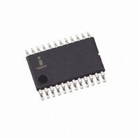
X9252TV24IZ-2.7 Intersil, X9252TV24IZ-2.7 Datasheet - Page 10

X9252TV24IZ-2.7
Manufacturer Part Number
X9252TV24IZ-2.7
Description
IC POT DGTL QUAD 100KOHM 24TSSOP
Manufacturer
Intersil
Series
XDCP™r
Datasheet
1.X9252YV24IZ-2.7.pdf
(20 pages)
Specifications of X9252TV24IZ-2.7
Taps
256
Resistance (ohms)
100K
Number Of Circuits
4
Temperature Coefficient
300 ppm/°C Typical
Memory Type
Non-Volatile
Interface
I²C, 2-Wire Serial
Voltage - Supply
2.7 V ~ 5.5 V
Operating Temperature
-40°C ~ 85°C
Mounting Type
Surface Mount
Package / Case
24-TSSOP
Resistance In Ohms
100K
Lead Free Status / RoHS Status
Lead free / RoHS Compliant
Available stocks
Company
Part Number
Manufacturer
Quantity
Price
Part Number:
X9252TV24IZ-2.7
Manufacturer:
INTERSIL
Quantity:
20 000
Serial Acknowledge
An ACK (Acknowledge), is a software convention used to
indicate a successful data transfer. The transmitting device,
either master or slave, releases the bus after transmitting
eight bits. During the ninth clock cycle, the receiver pulls the
SDA line LOW to acknowledge the reception of the eight bits
of data (See Figure 3).
The device responds with an ACK after recognition of a
START condition followed by a valid Slave Address byte. A
valid Slave Address byte must contain the Device Type
Identifier 0101, and the Device Address bits matching the
logic state of pins A2, A1, and A0 (See Figure 4).
If a write operation is selected, the device responds with an
ACK after the receipt of each subsequent eight-bit word.
In the read mode, the device transmits eight bits of data,
releases the SDA line, and then monitors the line for an
ACK. The device continues transmitting data if an ACK is
detected. The device terminates further data transmissions if
an ACK is not detected. The master must then issue a STOP
condition to place the device into a known state.
SDA Output from
SDA Output from
SCL from Master
Transmitter
SDA
SCL
Receiver
10
START
FIGURE 2. VALID DATA CHANGES, START, AND STOP CONDITIONS
START
FIGURE 3. ACKNOWLEDGE RESPONSE FROM RECEIVER
1
STABLE
DATA
X9252
CHANGE
DATA
Slave Address Byte
Following a START condition, the master must output a Slave
Address Byte (Refer to figure 4.). This byte includes three parts:
- The four MSBs (SA7-SA4) are the Device Type Identifier,
- The next three bits (SA3-SA1) are the Device Address bits
- The LSB (SA0) is the R/W bit. This bit defines the
SLAVE ADDRESS
which must always be set to 0101 in order to select the
X9252.
(AS2-AS0). To access any part of the X9252’s memory,
the value of bits AS2, AS1, and AS0 must correspond to
the logic levels at pins A2, A1, and A0 respectively.
operation to be performed on the device being
addressed. When the R/W bit is “1”, then a Read
operation is selected. A “0” selects a Write operation
SA7
STABLE
0
DATA
SA7-SA4
SA3-SA1
BIT(S)
FIGURE 4. SLAVE ADDRESS (SA) FORMAT
Device Type
SA0
SA6
Identifier
1
8
SA5
0
Device Type Identifier
Device Address
Read or Write Operation Select
SA4
1
STOP
ACK
SA3
AS2
9
DESCRIPTION
Address
Device
SA2
AS1
AS0
SA1
Read or
November 14, 2005
Write
R/W
SA0
FN8167.2
.


