X9252TV24IZ-2.7 Intersil, X9252TV24IZ-2.7 Datasheet - Page 7
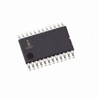
X9252TV24IZ-2.7
Manufacturer Part Number
X9252TV24IZ-2.7
Description
IC POT DGTL QUAD 100KOHM 24TSSOP
Manufacturer
Intersil
Series
XDCP™r
Datasheet
1.X9252YV24IZ-2.7.pdf
(20 pages)
Specifications of X9252TV24IZ-2.7
Taps
256
Resistance (ohms)
100K
Number Of Circuits
4
Temperature Coefficient
300 ppm/°C Typical
Memory Type
Non-Volatile
Interface
I²C, 2-Wire Serial
Voltage - Supply
2.7 V ~ 5.5 V
Operating Temperature
-40°C ~ 85°C
Mounting Type
Surface Mount
Package / Case
24-TSSOP
Resistance In Ohms
100K
Lead Free Status / RoHS Status
Lead free / RoHS Compliant
Available stocks
Company
Part Number
Manufacturer
Quantity
Price

Part Number:
X9252TV24IZ-2.7
Manufacturer:
INTERSIL
Quantity:
20 000


Increment/Decrement Timing
High-Voltage Write Cycle Timing
NOTES:
XDCP Timing
t
1. Absolute linearity is utilized to determine actual wiper voltage versus expected voltage = [V(R
2. Relative linearity is a measure of the error in step size between taps = [V(R
3. 1 Ml = Minimum Increment = [V(R
4. Typical values are for T
5. This parameter is not 100% tested.
6. Ratiometric temperature coefficient = (V(R
7. Measured with wiper at tap position 255, R
8. t
9. The recommended power up sequence is to apply V
WRL
(Notes 5, 8)
DS0, DS1
SYMBOL
SYMBOL
V(R
255.
STOP condition at the end of a write sequence of a 2-wire interface write operation, or from the rising edge of CS of a valid “Store” operation of
the Up/Down interface, to the end of the self-timed internal nonvolatile write cycle.
for the DCP do not fully apply until t
store, bring the CS pin high before or concurrently with the V
WC
t
WC
(Note 5) SCL rising edge to wiper code changed, wiper response time after instruction
SCL
U/D
CS
R
W(n)(expected)
is the minimum cycle time to be allowed for any nonvolatile write by the user, unless Acknowledge Polling is used. It is the time from a valid
W
t
Non-volatile write cycle time
issued (all load instructions)
CI
t
) = n(V(R
IW
A
= 25°C and nominal supply voltage.
H
t
)-V(R
IL
7
t
ID
t
CYC
H
L
))/255 + V(R
)-V(R
D
after V
t
L
IH
)]/255.
W
L
)
CC
grounded, using test circuit.
T1(n)
PARAMETER
PARAMETER
L
reaches its final value. In order to prevent unwanted tap position changes, or an inadvertant
), with n from 0 to 255.
-V(R
t
DI
CC
W
/V
t
)
IC
T2(n)
SS
MI
first, then the potentiometer voltages. During power up, the data sheet parameters
CC
)/[V(R
(3)
X9252
pin on power up.
W
)
T1(n)
W(n+1)
(T1-T2)] x 10
t
CPHS
)-(V(R
W(n)
6
, with T1 & T2 being 2 temperatures, and n from 0 to
t
F
) + MI)]/MI, with n from 0 to 254
W(n)(actual)
90%
10%
TYP
MIN
5
5
)-V(R
90%
W(n)(expected)
t
R
MAX
MAX
20
10
t
CPHNS
)]/MI
November 14, 2005
UNITS
UNITS
ms
µs
FN8167.2
Related parts for X9252TV24IZ-2.7
Image
Part Number
Description
Manufacturer
Datasheet
Request
R

Part Number:
Description:
IC DCP QUAD 100K 256TAP 24-TSSOP
Manufacturer:
Intersil
Datasheet:

Part Number:
Description:
Intersil Corporation [CMOS Serial Controller Interface]
Manufacturer:
Intersil Corporation
Datasheet:
Part Number:
Description:
Manufacturer:
Intersil Corporation
Datasheet:
Part Number:
Description:
357-036-542-201 CARDEDGE 36POS DL .156 BLK LOPRO
Manufacturer:
Intersil Corporation
Datasheet:
Part Number:
Description:
1024-Word x 4-Bit LSI Static RAM
Manufacturer:
Intersil Corporation
Datasheet:
Part Number:
Description:
General Purpose NPN Transistor Arrays FN341.4
Manufacturer:
Intersil Corporation
Datasheet:
Part Number:
Description:
CMOS 16-Bit Microprocessor
Manufacturer:
Intersil Corporation
Datasheet:
Part Number:
Description:
Manufacturer:
Intersil Corporation
Datasheet:
Part Number:
Description:
Manufacturer:
Intersil Corporation
Datasheet:
Part Number:
Description:
Manufacturer:
Intersil Corporation
Datasheet:
Part Number:
Description:
Manufacturer:
Intersil Corporation
Datasheet:
Part Number:
Description:
CMOS 6-Bit Latch and Decoder Memory Interfaces
Manufacturer:
Intersil Corporation
Datasheet:
Part Number:
Description:
CA3046General Purpose NPN Transistor Arrays
Manufacturer:
Intersil Corporation
Datasheet:
Part Number:
Description:
Manufacturer:
Intersil Corporation
Datasheet:
Part Number:
Description:
TR909 DLC/FLC SLIC with Low Power Standby
Manufacturer:
Intersil Corporation
Datasheet: