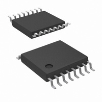
DAC108S085CIMT/NOPB National Semiconductor, DAC108S085CIMT/NOPB Datasheet - Page 7

DAC108S085CIMT/NOPB
Manufacturer Part Number
DAC108S085CIMT/NOPB
Description
IC DAC 10BIT OCTAL R-R 16-TSSOP
Manufacturer
National Semiconductor
Series
PowerWise®r
Datasheet
1.DAC108S085CISQNOPB.pdf
(24 pages)
Specifications of DAC108S085CIMT/NOPB
Settling Time
4.5µs
Number Of Bits
10
Data Interface
Serial
Number Of Converters
8
Voltage Supply Source
Single Supply
Power Dissipation (max)
4.85mW
Operating Temperature
-40°C ~ 125°C
Mounting Type
Surface Mount
Package / Case
16-TSSOP
For Use With
DAC108S085EB - BOARD EVALUATION FOR DAC108S085
Lead Free Status / RoHS Status
Lead free / RoHS Compliant
Other names
DAC108S085CIMT
Available stocks
Company
Part Number
Manufacturer
Quantity
Price
Company:
Part Number:
DAC108S085CIMT/NOPB
Manufacturer:
NSC
Quantity:
1 563
Part Number:
DAC108S085CIMT/NOPB
Manufacturer:
TI/德州仪器
Quantity:
20 000
Note 1: Absolute Maximum Ratings indicate limits beyond which damage to the device may occur. Operating Ratings indicate conditions for which the device is
functional, but do not guarantee specific performance limits. For guaranteed specifications and test conditions, see the Electrical Characteristics. The guaranteed
specifications apply only for the test conditions listed. Some performance characteristics may degrade when the device is not operated under the listed test
conditions. Operation of the device beyond the maximum Operating Ratings is not recommended.
Note 2: All voltages are measured with respect to GND = 0V, unless otherwise specified.
Note 3: When the input voltage at any pin exceeds 5.5V or is less than GND, the current at that pin should be limited to 10 mA. The 30 mA maximum package
input current rating limits the number of pins that can safely exceed the power supplies with an input current of 10 mA to three.
Note 4: The absolute maximum junction temperature (T
max) for this device is 150°C. The maximum allowable power dissipation is dictated by T
max, the
J
J
) / θ
junction-to-ambient thermal resistance (θ
), and the ambient temperature (T
), and can be calculated using the formula P
MAX = (T
max − T
. The values
JA
A
D
J
A
JA
for maximum power dissipation will be reached only when the device is operated in a severe fault condition (e.g., when input or output pins are driven beyond
the operating ratings, or the power supply polarity is reversed). Such conditions should always be avoided.
Note 5: Human body model is 100 pF capacitor discharged through a 1.5 kΩ resistor. Machine model is 220 pF discharged through 0 Ω. Charge device model
simulates a pin slowly acquiring charge (such as from a device sliding down the feeder in an automated assembler) then rapidly being discharged.
Note 6: Reflow temperature profiles are different for lead-free packages.
Note 7: The inputs are protected as shown below. Input voltage magnitudes up to 5.5V, regardless of V
, will not cause errors in the conversion result. For
A
example, if V
is 3V, the digital input pins can be driven with a 5V logic device.
A
30031204
Note 8: Test limits are guaranteed to National's AOQL (Average Outgoing Quality Level).
Note 9: This parameter is guaranteed by design and/or characterization and is not tested in production.
Note 10: This parameter does not represent a condition which the DAC can sustain continuously. See the continuous output current specification for the maximum
DAC output current per channel.
Timing Diagrams
30031206
FIGURE 1. Serial Timing Diagram
7
www.national.com


