AD5390BSTZ-5 Analog Devices Inc, AD5390BSTZ-5 Datasheet - Page 17
AD5390BSTZ-5
Manufacturer Part Number
AD5390BSTZ-5
Description
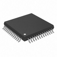
IC DAC 14BIT I2C 16CH 52-LQFP
Manufacturer
Analog Devices Inc
Specifications of AD5390BSTZ-5
Data Interface
I²C, Serial
Design Resources
8 to 16 Channels of Programmable Voltage with Excellent Temperature Drift Performance Using AD5390/1/2 (CN0029) AD5390/91/92 Channel Monitor Function (CN0030)
Settling Time
8µs
Number Of Bits
14
Number Of Converters
16
Voltage Supply Source
Single Supply
Power Dissipation (max)
35mW
Operating Temperature
-40°C ~ 85°C
Mounting Type
Surface Mount
Package / Case
52-LQFP
Resolution (bits)
14bit
Sampling Rate
125kSPS
Input Channel Type
Serial
Supply Voltage Range - Analogue
4.5V To 5.5V
Supply Voltage Range - Digital
2.7V To 5.5V
Lead Free Status / RoHS Status
Lead free / RoHS Compliant
For Use With
EVAL-AD5390EBZ - BOARD EVALUATION FOR AD5390
Lead Free Status / RoHS Status
Lead free / RoHS Compliant, Lead free / RoHS Compliant
Available stocks
Company
Part Number
Manufacturer
Quantity
Price
Company:

Part Number:
AD5390BSTZ-5
Manufacturer:
Analog Devices Inc
Quantity:
10 000


TERMINOLOGY
Relative Accuracy or Endpoint Linearity (INL)
A measure of the maximum deviation from a straight line
passing through the endpoints of the DAC transfer function.
It is measured after adjusting for zero-scale error and full-scale
error and is expressed in least significant bits (LSBs).
Differential Nonlinearity (DNL)
The difference between the measured change and the ideal
1 LSB change between any two adjacent codes. A specified
differential nonlinearity of 1 LSB maximum ensures mono-
tonicity.
Zero-Scale Error
The error in the DAC output voltage when all 0s are loaded
into the DAC register. Ideally, with all 0s loaded to the DAC
and m = all 1s, c = 2
Zero-scale error is a measure of the difference between VOUT
(actual) and VOUT (ideal) expressed in mV. It is mainly caused
by offsets in the output amplifier.
Offset Error
A measure of the difference between VOUT (actual) and VOUT
(ideal) expressed in mV in the linear region of the transfer
function. Offset error is measured on the AD539x-5 with code
32 loaded in the DAC register and with code 64 loaded in the
DAC register on the AD539x-3.
Gain Error
The deviation in slope of the DAC transfer characteristic from
ideal and is expressed in % FSR with the DAC output unloaded.
Gain error is specified in the linear region of the output range
between VOUT = 10 mV and VOUT = AV
DC Crosstalk
The dc change in the output level of one DAC at midscale in
response to a full-scale code (all 0s to all 1s and vice versa) and
the output change of all other DACs. It is expressed in LSBs.
n−1
, VOUT
(Zero-Scale)
= 0 V.
DD
− 50 mV.
Rev. C | Page 17 of 40
DC Output Impedance
The effective output source resistance. It is dominated by
package lead resistance.
Output Voltage Settling Time
The amount of time it takes for the output of a DAC to settle
to a specified level for a ¼ to ¾ full-scale input change. It is
measured from the rising edge of BUSY .
Digital-to-Analog Glitch Energy
The amount of energy injected into the analog output at the
major code transition. It is specified as the area of the glitch in
nV-s. It is measured by toggling the DAC register data between
0x1FFF and 0x2000.
DAC-to-DAC Crosstalk
The glitch impulse that appears at the output of one DAC due to
both the digital change and subsequent analog output change at
another DAC. The victim channel is loaded with midscale, and
DAC-to-DAC crosstalk is specified in nV-s.
Digital Crosstalk
The glitch impulse transferred to the output of one converter
due to a change in the DAC register code of another converter
is defined as the digital crosstalk and is specified in nV-s.
Digital Feedthrough
When the device is not selected, high frequency logic activity
on the device’s digital inputs can be capacitively coupled both
across and through the device to show up as noise on the VOUT
pins. It can also be coupled along the supply and ground lines.
This noise is digital feedthrough.
Output Noise Spectral Density
This is a measure of internally generated random noise. Random
noise is characterized as a spectral density (voltage per √Hz).
It is measured by loading all DACs to midscale and measuring
noise at the output. It is measured in nV/(Hz)
bandwidth at 10 kHz.
AD5390/AD5391/AD5392
1/2
in a 1 Hz
Related parts for AD5390BSTZ-5
Image
Part Number
Description
Manufacturer
Datasheet
Request
R

Part Number:
Description:
Wideband Dual-Channel Linear Multiplier/Divider
Manufacturer:
AD [Analog Devices]
Datasheet:

Part Number:
Description:
±1.7g Dual-Axis IMEMS Accelerometer Evaluation Board
Manufacturer:
Analog Devices Inc
Datasheet:

Part Number:
Description:
Inertial Sensor Evaluation System
Manufacturer:
Analog Devices Inc
Datasheet:
Part Number:
Description:
Manufacturer:
Analog Devices Inc
Datasheet:
Part Number:
Description:
Manufacturer:
Analog Devices Inc
Datasheet:
Part Number:
Description:
Manufacturer:
Analog Devices Inc
Datasheet:
Part Number:
Description:
Manufacturer:
Analog Devices Inc
Datasheet:
Part Number:
Description:
Manufacturer:
Analog Devices Inc
Datasheet:
Part Number:
Description:
Manufacturer:
Analog Devices Inc
Datasheet:
Part Number:
Description:
Manufacturer:
Analog Devices Inc
Datasheet:
Part Number:
Description:
Manufacturer:
Analog Devices Inc
Datasheet:
Part Number:
Description:
Manufacturer:
Analog Devices Inc
Datasheet:
Part Number:
Description:
Manufacturer:
Analog Devices Inc
Datasheet: