AD5390BSTZ-5 Analog Devices Inc, AD5390BSTZ-5 Datasheet - Page 7
AD5390BSTZ-5
Manufacturer Part Number
AD5390BSTZ-5
Description
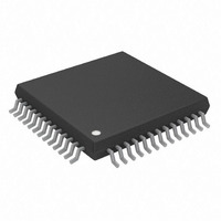
IC DAC 14BIT I2C 16CH 52-LQFP
Manufacturer
Analog Devices Inc
Specifications of AD5390BSTZ-5
Data Interface
I²C, Serial
Design Resources
8 to 16 Channels of Programmable Voltage with Excellent Temperature Drift Performance Using AD5390/1/2 (CN0029) AD5390/91/92 Channel Monitor Function (CN0030)
Settling Time
8µs
Number Of Bits
14
Number Of Converters
16
Voltage Supply Source
Single Supply
Power Dissipation (max)
35mW
Operating Temperature
-40°C ~ 85°C
Mounting Type
Surface Mount
Package / Case
52-LQFP
Resolution (bits)
14bit
Sampling Rate
125kSPS
Input Channel Type
Serial
Supply Voltage Range - Analogue
4.5V To 5.5V
Supply Voltage Range - Digital
2.7V To 5.5V
Lead Free Status / RoHS Status
Lead free / RoHS Compliant
For Use With
EVAL-AD5390EBZ - BOARD EVALUATION FOR AD5390
Lead Free Status / RoHS Status
Lead free / RoHS Compliant, Lead free / RoHS Compliant
Available stocks
Company
Part Number
Manufacturer
Quantity
Price
Company:

Part Number:
AD5390BSTZ-5
Manufacturer:
Analog Devices Inc
Quantity:
10 000


AD5390-3/AD5391-3/AD5392-3 SPECIFICATIONS
AV
unless otherwise noted.
Table 4.
Parameter
ACCURACY
REFERENCE INPUT/OUTPUT
OUTPUT CHARACTERISTICS
MONITOR OUTPUT PIN
LOGIC INPUTS
Resolution
Relative Accuracy
Differential Nonlinearity
Zero-Scale Error
Offset Error
Offset Error TC
Gain Error
Gain Temperature Coefficient
DC Crosstalk
Reference Input
Reference Output
Output Voltage Range
Short-Circuit Current
Load Current
Capacitive Load Stability
DC Output Impedance
Output Impedance
Three-State Leakage Current
V
V
Input Current
Pin Capacitance
Logic Inputs (SCL, SDA Only)
Glitch Rejection
DD
IH
IL
, Input Low Voltage
Reference Input Voltage
DC Input Impedance
Input Current
Reference Range
Output Voltage
Reference TC
Output Impedance
R
R
V
V
I
V
, Input High Voltage
IN
= 2.7 V to 3.6 V; DV
L
L
IH
IL
HYST
, Input Leakage Current
, Input Low Voltage
= ∞
= 5 kΩ
, Input High Voltage
, Input Hysteresis
2
2
3
2
4
DD
2
= 2.7 V to 5.5 V; AGND = DGND = 0 V; REFIN = 1.25 V external. All specifications T
2
AD5390-3
AD5392-3
14
±4
−1/+2
4
±4
±5
±0.024
±0.1
2
0.5
1.25
1
±1
1 V to AV
1.245/1.255
2.47/2.53
±10
±15
2.2
0/AV
40
±1
200
1000
0.5
500
100
2
0.8
±10
10
0.7 DV
0.3 DV
±1
0.05 DV
50
DD
DD
DD
DD
DD
1
1
/2
AD5391-3
12
±1
±1
4
±4
±5
±0.024
±0.1
2
0.5
1.25
1
±1
1 V to AV
1.245/1.255
2.47/2.53
±10
±15
2.2
0/AV
40
±1
200
1000
0.5
500
100
2
0.8
±10
10
0.7 DV
0.3 DV
±1
0.05 DV
50
DD
Rev. C | Page 7 of 40
DD
DD
DD
DD
1
/2
Unit
Bits
LSB max
LSB max
mV max
mV max
μV/°C typ
% FSR max
% FSR max
ppm FSR/°C typ
mV max
V
MΩ min
μA max
V min/max
V min/max
V min/max
ppm max
ppm max
kΩ typ
V min/max
mA max
mA max
pF max
pF max
Ω max
Ω typ
nA typ
V min
V max
μA max
pF max
V min
V max
μA max
V min
ns max
Test Conditions/Comments
Guaranteed monotonic over temperature
Measured at code 64 in the linear region
At 25°C
T
±1% for specified performance
Typically 100 MΩ
Typically ±30 nA
Enabled via internal/external bit in control
register; REF select bit in control register
selects the reference voltage
At ambient, optimized for 1.25 V operation
At ambient when 2.5 V reference is selected
Temperature range: 25°C to 85°C
Temperature range: −40°C to +85°C
DV
Total for all pins. T
SMBus-compatible at DV
SMBus-compatible at DV
Input filtering suppresses noise spikes <50 ns
MIN
DD
to T
= 2.7 V to 5.5 V
AD5390/AD5391/AD5392
MAX
A
= T
MIN
MIN
DD
DD
to T
to T
< 3.6 V
< 3.6 V
MAX
MAX
,
Related parts for AD5390BSTZ-5
Image
Part Number
Description
Manufacturer
Datasheet
Request
R

Part Number:
Description:
Wideband Dual-Channel Linear Multiplier/Divider
Manufacturer:
AD [Analog Devices]
Datasheet:

Part Number:
Description:
±1.7g Dual-Axis IMEMS Accelerometer Evaluation Board
Manufacturer:
Analog Devices Inc
Datasheet:

Part Number:
Description:
Inertial Sensor Evaluation System
Manufacturer:
Analog Devices Inc
Datasheet:
Part Number:
Description:
Manufacturer:
Analog Devices Inc
Datasheet:
Part Number:
Description:
Manufacturer:
Analog Devices Inc
Datasheet:
Part Number:
Description:
Manufacturer:
Analog Devices Inc
Datasheet:
Part Number:
Description:
Manufacturer:
Analog Devices Inc
Datasheet:
Part Number:
Description:
Manufacturer:
Analog Devices Inc
Datasheet:
Part Number:
Description:
Manufacturer:
Analog Devices Inc
Datasheet:
Part Number:
Description:
Manufacturer:
Analog Devices Inc
Datasheet:
Part Number:
Description:
Manufacturer:
Analog Devices Inc
Datasheet:
Part Number:
Description:
Manufacturer:
Analog Devices Inc
Datasheet:
Part Number:
Description:
Manufacturer:
Analog Devices Inc
Datasheet: