AD5390BSTZ-5 Analog Devices Inc, AD5390BSTZ-5 Datasheet - Page 29
AD5390BSTZ-5
Manufacturer Part Number
AD5390BSTZ-5
Description
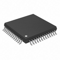
IC DAC 14BIT I2C 16CH 52-LQFP
Manufacturer
Analog Devices Inc
Specifications of AD5390BSTZ-5
Data Interface
I²C, Serial
Design Resources
8 to 16 Channels of Programmable Voltage with Excellent Temperature Drift Performance Using AD5390/1/2 (CN0029) AD5390/91/92 Channel Monitor Function (CN0030)
Settling Time
8µs
Number Of Bits
14
Number Of Converters
16
Voltage Supply Source
Single Supply
Power Dissipation (max)
35mW
Operating Temperature
-40°C ~ 85°C
Mounting Type
Surface Mount
Package / Case
52-LQFP
Resolution (bits)
14bit
Sampling Rate
125kSPS
Input Channel Type
Serial
Supply Voltage Range - Analogue
4.5V To 5.5V
Supply Voltage Range - Digital
2.7V To 5.5V
Lead Free Status / RoHS Status
Lead free / RoHS Compliant
For Use With
EVAL-AD5390EBZ - BOARD EVALUATION FOR AD5390
Lead Free Status / RoHS Status
Lead free / RoHS Compliant, Lead free / RoHS Compliant
Available stocks
Company
Part Number
Manufacturer
Quantity
Price
Company:

Part Number:
AD5390BSTZ-5
Manufacturer:
Analog Devices Inc
Quantity:
10 000


2-BYTE MODE
The 2-byte mode lets the user update channels sequentially
following initialization of this mode. The device address byte is
required only once and the address pointer is configured for
autoincrement or burst mode.
The user must begin with an address byte (R/ W = 0), after
which the DAC acknowledges that it is prepared to receive data
by pulling SDA low. The address byte is followed by a specific
pointer byte (0xFF), which initiates the burst mode of opera-
tion. The address pointer initializes to Channel 0 and the data
following the pointer is loaded to Channel 0. The address
pointer automatically increments to the next address.
SDA
SDA
SDA
SDA
SCL
SCL
SCL
SCL
CONDITION
MASTER
START
BY
REG1
REG1
1
REG1
REG0
REG0
0
REG0
MSB
MOST SIGNIFICANT DATA BYTE
MSB
MOST SIGNIFICANT DATA BYTE
1
MOST SIGNIFICANT DATA BYTE
MSB
ADDRESS BYTE
0
1
AD1
AD0
CHANNEL N DATA FOLLOWED BY STOP
Figure 36. 2-Byte Mode I
LSB
LSB
R/W
CHANNEL 0 DATA
CHANNEL 1 DATA
CONVERTER
CONVERTER
CONVERTER
LSB
Rev. C | Page 29 of 40
ACK
BY
ACK
BY
ACK
CONVERTER
BY
ACK
BY
A7 = 1 A6 = 1 A5 = 1 A4 = 1 A3 = 1 A2 = 1 A1 = 1 A0 = 1
MSB
MSB
MSB
2
C Write Operation
MSB
The REG0 and REG1 bits in the data byte determine the register
to be updated. In this mode, following the initialization, only
the two data bytes are required to update a channel. The
channel address automatically increments from Address 0 to
the final address and then returns to the normal 3-byte mode
of operation. This mode allows transmission of data to all
channels in one block and reduces the software overhead in
configuring all channels. A STOP condition at any time exits
this mode. Toggle mode of operation is not supported in
2-byte mode. Figure 36 shows a typical configuration.
LEAST SIGNIFICANT DATA BYTE
LEAST SIGNIFICANT DATA BYTE
LEAST SIGNIFICANT DATA BYTE
POINTER BYTE
AD5390/AD5391/AD5392
CONVERTER
CONVERTER
LSB
LSB
CONVERTER
ACK
ACK
CONVERTER
ACK
BY
BY
LSB
BY
ACK
BY
CONDITION
MASTER
STOP
BY
Related parts for AD5390BSTZ-5
Image
Part Number
Description
Manufacturer
Datasheet
Request
R

Part Number:
Description:
Wideband Dual-Channel Linear Multiplier/Divider
Manufacturer:
AD [Analog Devices]
Datasheet:

Part Number:
Description:
±1.7g Dual-Axis IMEMS Accelerometer Evaluation Board
Manufacturer:
Analog Devices Inc
Datasheet:

Part Number:
Description:
Inertial Sensor Evaluation System
Manufacturer:
Analog Devices Inc
Datasheet:
Part Number:
Description:
Manufacturer:
Analog Devices Inc
Datasheet:
Part Number:
Description:
Manufacturer:
Analog Devices Inc
Datasheet:
Part Number:
Description:
Manufacturer:
Analog Devices Inc
Datasheet:
Part Number:
Description:
Manufacturer:
Analog Devices Inc
Datasheet:
Part Number:
Description:
Manufacturer:
Analog Devices Inc
Datasheet:
Part Number:
Description:
Manufacturer:
Analog Devices Inc
Datasheet:
Part Number:
Description:
Manufacturer:
Analog Devices Inc
Datasheet:
Part Number:
Description:
Manufacturer:
Analog Devices Inc
Datasheet:
Part Number:
Description:
Manufacturer:
Analog Devices Inc
Datasheet:
Part Number:
Description:
Manufacturer:
Analog Devices Inc
Datasheet: