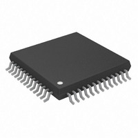
AD5390BSTZ-5 Analog Devices Inc, AD5390BSTZ-5 Datasheet - Page 6

AD5390BSTZ-5
Manufacturer Part Number
AD5390BSTZ-5
Description
IC DAC 14BIT I2C 16CH 52-LQFP
Manufacturer
Analog Devices Inc
Specifications of AD5390BSTZ-5
Data Interface
I²C, Serial
Design Resources
8 to 16 Channels of Programmable Voltage with Excellent Temperature Drift Performance Using AD5390/1/2 (CN0029) AD5390/91/92 Channel Monitor Function (CN0030)
Settling Time
8µs
Number Of Bits
14
Number Of Converters
16
Voltage Supply Source
Single Supply
Power Dissipation (max)
35mW
Operating Temperature
-40°C ~ 85°C
Mounting Type
Surface Mount
Package / Case
52-LQFP
Resolution (bits)
14bit
Sampling Rate
125kSPS
Input Channel Type
Serial
Supply Voltage Range - Analogue
4.5V To 5.5V
Supply Voltage Range - Digital
2.7V To 5.5V
Lead Free Status / RoHS Status
Lead free / RoHS Compliant
For Use With
EVAL-AD5390EBZ - BOARD EVALUATION FOR AD5390
Lead Free Status / RoHS Status
Lead free / RoHS Compliant, Lead free / RoHS Compliant
Available stocks
Company
Part Number
Manufacturer
Quantity
Price
Company:
Part Number:
AD5390BSTZ-5
Manufacturer:
Analog Devices Inc
Quantity:
10 000
AD5390/AD5391/AD5392
AD5390-5/AD5391-5/AD5392-5 AC CHARACTERISTICS
AV
Table 3.
Parameter
DYNAMIC PERFORMANCE
1
2
Guaranteed by characterization, not production tested.
The slew rate can be adjusted via the current boost control bit in the DAC control register.
Output Voltage Settling Time
Output Noise (0.1 Hz to 10 Hz)
DD
AD5390/AD5392
AD5391
Slew rate
Digital-to-Analog Glitch Energy
Glitch Impulse Peak Amplitude
Channel-to-Channel Isolation
DAC-to-DAC Crosstalk
Digital Crosstalk
Digital Feedthrough
Output Noise Spectral Density
= 4.5 V to 5.5 V; DV
@ 1 kHz
@ 10 kHz
2
DD
= 2.7 V to 5.5 V; AGND = DGND = 0 V.
All
8
10
6
8
3
2
12
15
100
1
0.8
0.1
15
40
150
100
1
μs typ
μs typ
dB typ
Unit
μs max
μs max
V/μs typ
V/μs typ
nV-s typ
mV typ
nV-s typ
nV-s typ
nV-s typ
μV p-p typ
μV p-p typ
nV/(Hz)
nV/(Hz)
1/2
1/2
typ
typ
Rev. C | Page 6 of 40
Test Conditions/Comments
¼ scale to ¾ scale change settling to ±1 LSB
¼ scale to ¾ scale change settling to ±1 LSB
Boost mode on
Boost mode off
See the Terminology section
See the Terminology section
Effect of input bus activity on DAC output under test
External reference midscale loaded to DAC
Internal reference midscale loaded to DAC


