AD5390BSTZ-5 Analog Devices Inc, AD5390BSTZ-5 Datasheet - Page 38
AD5390BSTZ-5
Manufacturer Part Number
AD5390BSTZ-5
Description
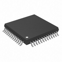
IC DAC 14BIT I2C 16CH 52-LQFP
Manufacturer
Analog Devices Inc
Specifications of AD5390BSTZ-5
Data Interface
I²C, Serial
Design Resources
8 to 16 Channels of Programmable Voltage with Excellent Temperature Drift Performance Using AD5390/1/2 (CN0029) AD5390/91/92 Channel Monitor Function (CN0030)
Settling Time
8µs
Number Of Bits
14
Number Of Converters
16
Voltage Supply Source
Single Supply
Power Dissipation (max)
35mW
Operating Temperature
-40°C ~ 85°C
Mounting Type
Surface Mount
Package / Case
52-LQFP
Resolution (bits)
14bit
Sampling Rate
125kSPS
Input Channel Type
Serial
Supply Voltage Range - Analogue
4.5V To 5.5V
Supply Voltage Range - Digital
2.7V To 5.5V
Lead Free Status / RoHS Status
Lead free / RoHS Compliant
For Use With
EVAL-AD5390EBZ - BOARD EVALUATION FOR AD5390
Lead Free Status / RoHS Status
Lead free / RoHS Compliant, Lead free / RoHS Compliant
Available stocks
Company
Part Number
Manufacturer
Quantity
Price
Company:

Part Number:
AD5390BSTZ-5
Manufacturer:
Analog Devices Inc
Quantity:
10 000


AD5390/AD5391/AD5392
12- and 14-bit resolution. Figure 45 shows a typical transmitter
architecture, in which the AD539x DACs can be used in the
following control circuits: I
(APC), peak power control (PPC), transmit gain control (TGC),
and audio level control (ALC). DACs are also required for
variable voltage attenuators, phase shifter control, and dc-
setpoint control in the overall amplifier design.
Process Control Applications
The AD539x-5 family is ideal for process control applications
because it offers a combination of 8 and 16 channels and 12-bit
and 14-bit resolution. These applications generally require
output voltage ranges of 0 V to 5 V ± 5 V, 0 V to 10 V ± 10 V,
and current sink and source functions. The AD539x-5 products
operate from a single 5 V supply and, therefore, require external
signal conditioning to achieve the output ranges described here.
Figure 46 shows configurations to achieve these output ranges.
The key advantages of using AD539x-5 products in these
applications are small package size, pin compatibility with the
ability to upgrade from 12 to 14 bits, integrated on-chip 2.5 V
reference with 10 ppm/°C maximum temperature coefficient,
and excellent accuracy specifications. The AD539x-5 family
contains an offset and gain register for each channel, so users
can perform system-level calibration on a per-channel basis.
SOURCE
AUDIO
Figure 45. Multistage Power Amplifier Control
ALC
EXCITER
PPC
BIAS
control, average power control
PHASE
SHIFT
AMPLIFIER
APC
POWER
I
BIAS
TGC
LOAD
50Ω
Rev. C | Page 38 of 40
0V TO 10V
Optical Transceivers
The AD539x-3 family of products are ideally suited to optical
transceiver applications. In 300-pin MSA applications, for
example, digital-to-analog converters are required to control the
laser power, APD bias, and modulator amplitude. Diagnostic
information is required as analog outputs from the module. The
AD539x-3 products offer a combination of 8/16 channels, a
resolution of 12/14 bits in a 64-lead LFCSP, and operate from a
supply voltage of 2.7 V to 5.5 V supply with internal reference.
The AD539x-3 parts also feature I
faces, making them ideal components for use in these applications.
Figure 47 shows a typical configuration in an optical transceiver
application.
RANGE
RANGE
10G LDD
PIN/APD
AND TIA
LASER
±10V
AND
1/4 OP4177
1/4 OP4177
1/4 OP747/
1/4 OP747/
Figure 46. Output Configurations for Process Control Applications
IRXP
IMODMON
IMPD
IBIASMON
4R
R
Figure 47. Optical Transceiver using the AD539x-3
BUS
I
3V
2
TIAs
C
4R
R
R
R
MUX
AIN
AV
DD
VOUT 3
VOUT 4
AD7994
CONTROLLER
SDA
AD539x-5
12-BIT
REFERENCE
ADC
REFIN
2.5V
SCL
VOUT 0
VOUT 1
VOUT 2
2
C-compatible and SPI inter-
0.1µF
SDA
SCL
REFOUT/REFIN
AD539x-3
DV
DD
AV
1/4 OP4177
1/4 OP747/
R
R
DD
VLSRBIAS
VLSRPWRMON
VXLOPMON
I
IMOD
BIAS
2R
2R
1/4 OP4177
1/4 OP747/
0V TO 5V
I SINK
R1
RANGE
RANGE
±5V
Related parts for AD5390BSTZ-5
Image
Part Number
Description
Manufacturer
Datasheet
Request
R

Part Number:
Description:
Wideband Dual-Channel Linear Multiplier/Divider
Manufacturer:
AD [Analog Devices]
Datasheet:

Part Number:
Description:
±1.7g Dual-Axis IMEMS Accelerometer Evaluation Board
Manufacturer:
Analog Devices Inc
Datasheet:

Part Number:
Description:
Inertial Sensor Evaluation System
Manufacturer:
Analog Devices Inc
Datasheet:
Part Number:
Description:
Manufacturer:
Analog Devices Inc
Datasheet:
Part Number:
Description:
Manufacturer:
Analog Devices Inc
Datasheet:
Part Number:
Description:
Manufacturer:
Analog Devices Inc
Datasheet:
Part Number:
Description:
Manufacturer:
Analog Devices Inc
Datasheet:
Part Number:
Description:
Manufacturer:
Analog Devices Inc
Datasheet:
Part Number:
Description:
Manufacturer:
Analog Devices Inc
Datasheet:
Part Number:
Description:
Manufacturer:
Analog Devices Inc
Datasheet:
Part Number:
Description:
Manufacturer:
Analog Devices Inc
Datasheet:
Part Number:
Description:
Manufacturer:
Analog Devices Inc
Datasheet:
Part Number:
Description:
Manufacturer:
Analog Devices Inc
Datasheet: