AD5390BSTZ-5 Analog Devices Inc, AD5390BSTZ-5 Datasheet - Page 33
AD5390BSTZ-5
Manufacturer Part Number
AD5390BSTZ-5
Description
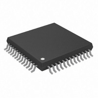
IC DAC 14BIT I2C 16CH 52-LQFP
Manufacturer
Analog Devices Inc
Specifications of AD5390BSTZ-5
Data Interface
I²C, Serial
Design Resources
8 to 16 Channels of Programmable Voltage with Excellent Temperature Drift Performance Using AD5390/1/2 (CN0029) AD5390/91/92 Channel Monitor Function (CN0030)
Settling Time
8µs
Number Of Bits
14
Number Of Converters
16
Voltage Supply Source
Single Supply
Power Dissipation (max)
35mW
Operating Temperature
-40°C ~ 85°C
Mounting Type
Surface Mount
Package / Case
52-LQFP
Resolution (bits)
14bit
Sampling Rate
125kSPS
Input Channel Type
Serial
Supply Voltage Range - Analogue
4.5V To 5.5V
Supply Voltage Range - Digital
2.7V To 5.5V
Lead Free Status / RoHS Status
Lead free / RoHS Compliant
For Use With
EVAL-AD5390EBZ - BOARD EVALUATION FOR AD5390
Lead Free Status / RoHS Status
Lead free / RoHS Compliant, Lead free / RoHS Compliant
Available stocks
Company
Part Number
Manufacturer
Quantity
Price
Company:

Part Number:
AD5390BSTZ-5
Manufacturer:
Analog Devices Inc
Quantity:
10 000


Table 27 shows the control register contents of the AD5391. Table 28 provides bit descriptions. Note that REG1 = REG0 = 0,
A3 to A0 = 1100, and DB13 to DB0 contain the control register data.
Table 27. AD5391 Control Register Contents
MSB
CR11
Table 28. AD5391 Bit Descriptions
Bit
CR11
CR10
CR9
CR8
CR7
CR6
CR5 to CR2
CR1 to CR0
CR10
Description
Power-Down Status. This bit is used to configure the output amplifier state in power-down mode.
CR11 = 1: Amplifier output is high impedance (default on power-up).
CR11 = 0: Amplifier output is 100 kΩ to ground.
REF Select. This bit selects the operating internal reference for the AD5391. CR10 is programmed as follows:
CR10 = 1: Internal reference is 2.5 V (AD5391-5 default). Recommended operating reference for AD5391-5.
CR10 = 0: Internal reference is 1.25 V (AD5391-3 default). Recommended operating reference for AD5391-3.
Current Boost Control. This bit is used to boost the current in the output amplifier, thus altering its slew rate. This bit is
configured as follows:
CR9 = 1: Boost mode on. This maximizes the bias current in the output amplifier, optimizing its slew rate but increasing
the power dissipation.
CR9 = 0: Boost mode off (default on power-up). This reduces the bias current in the output amplifier and reduces the overall
power consumption.
Internal/External Reference. This bits determines if the DAC uses its internal reference or an external reference.
CR8 = 1: Internal reference enabled. Reference output depends on data loaded to CR10.
CR8 = 0: External reference selected (default on power-up).
Channel Monitor Enable (see Table 24).
CR7 = 1: Monitor enabled. This enables the channel monitor function. Following a write to the monitor channel in
the SFR register, the selected channel output is routed to the MON_OUT pin.
CR7 = 0: Monitor disabled (default on power-up). When monitor is disabled, the MON_OUT pin is three-stated.
Thermal Monitor Function. When enabled, this function is used to monitor the internal die temperature of the AD5391,
when enabled. The thermal monitor powers down the output amplifiers when the temperature exceeds 130°C. This function
can be used to protect the device in cases where the power dissipation of the device may be exceeded, if a number of
output channels are simultaneously short circuited. A soft power-up re-enables the output amplifiers if the die temperature
has dropped below 130°C.
CR6 = 1: Thermal monitor enabled.
CR6 = 0: Thermal monitor disabled (default on power-up).
Don’t Care.
Toggle Function Enable. This function lets the user toggle the output between two codes loaded to the A and B register for
each DAC. Control Register Bit CR1 and Bit CR0 are used to enable individual groups of eight channels for operation in
toggle mode on the AD5391, as follows:
CR1
CR0
Logic 1 written to any bit enables a group of channels and Logic 0 disables a group. LDAC is used to toggle between the two
registers.
Group 1
Group 0
CR9
Channel 8 to Channel 15
Channel 0 to Channel 7
CR8
CR7
Rev. C | Page 33 of 40
CR6
CR5
CR4
CR3
AD5390/AD5391/AD5392
CR2
CR1
LSB
CR0
Related parts for AD5390BSTZ-5
Image
Part Number
Description
Manufacturer
Datasheet
Request
R

Part Number:
Description:
Wideband Dual-Channel Linear Multiplier/Divider
Manufacturer:
AD [Analog Devices]
Datasheet:

Part Number:
Description:
±1.7g Dual-Axis IMEMS Accelerometer Evaluation Board
Manufacturer:
Analog Devices Inc
Datasheet:

Part Number:
Description:
Inertial Sensor Evaluation System
Manufacturer:
Analog Devices Inc
Datasheet:
Part Number:
Description:
Manufacturer:
Analog Devices Inc
Datasheet:
Part Number:
Description:
Manufacturer:
Analog Devices Inc
Datasheet:
Part Number:
Description:
Manufacturer:
Analog Devices Inc
Datasheet:
Part Number:
Description:
Manufacturer:
Analog Devices Inc
Datasheet:
Part Number:
Description:
Manufacturer:
Analog Devices Inc
Datasheet:
Part Number:
Description:
Manufacturer:
Analog Devices Inc
Datasheet:
Part Number:
Description:
Manufacturer:
Analog Devices Inc
Datasheet:
Part Number:
Description:
Manufacturer:
Analog Devices Inc
Datasheet:
Part Number:
Description:
Manufacturer:
Analog Devices Inc
Datasheet:
Part Number:
Description:
Manufacturer:
Analog Devices Inc
Datasheet: