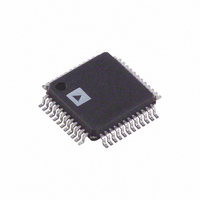
AD9763AST Analog Devices Inc, AD9763AST Datasheet - Page 21

AD9763AST
Manufacturer Part Number
AD9763AST
Description
IC DAC 10BIT DUAL 125MSPS 48LQFP
Manufacturer
Analog Devices Inc
Series
TxDAC+®r
Datasheet
1.AD9763ASTZ.pdf
(44 pages)
Specifications of AD9763AST
Rohs Status
RoHS non-compliant
Settling Time
35ns
Number Of Bits
10
Data Interface
Parallel
Number Of Converters
2
Voltage Supply Source
Analog and Digital
Power Dissipation (max)
450mW
Operating Temperature
-40°C ~ 85°C
Mounting Type
Surface Mount
Package / Case
48-LQFP
For Use With
AD9763-EBZ - BOARD EVAL FOR AD9763
Available stocks
Company
Part Number
Manufacturer
Quantity
Price
Company:
Part Number:
AD9763AST
Manufacturer:
AD
Quantity:
1 831
Company:
Part Number:
AD9763AST
Manufacturer:
ALTERA
Quantity:
591
Company:
Part Number:
AD9763ASTZ
Manufacturer:
ADI
Quantity:
180
Company:
Part Number:
AD9763ASTZ
Manufacturer:
Analog Devices Inc
Quantity:
10 000
Part Number:
AD9763ASTZ
Manufacturer:
ADI/亚德诺
Quantity:
20 000
Company:
Part Number:
AD9763ASTZRL
Manufacturer:
Analog Devices Inc
Quantity:
10 000
Part Number:
AD9763ASTZRL
Manufacturer:
ADI/亚德诺
Quantity:
20 000
THEORY OF OPERATION
FUNCTIONAL DESCRIPTION
Figure 58 shows a simplified block diagram of the AD9763/
AD9765/AD9767. The AD9763/AD9765/AD9767 consist of
two DACs, each one with its own independent digital control
logic and full-scale output current control. Each DAC contains
a PMOS current source array capable of providing up to 20 mA
of full-scale current (I
The array is divided into 31 equal currents that make up the five
most significant bits (MSBs). The next four bits, or middle bits,
consist of 15 equal current sources whose value is 1/16th of an
MSB current source. The remaining LSB is a binary weighted
fraction of the middle bit current sources. Implementing the
middle and lower bits with current sources, instead of an R-2R
ladder, enhances the dynamic performance for multitone or low
amplitude signals and helps maintain the high output impedance
of each DAC (that is, >100 kΩ).
I
NOTES
1. IN THIS CONFIGURATION, THE 22nF CAPACITOR AND 256Ω RESISTOR ARE NOT REQUIRED BECAUSE R
REF
R
DCOM1/DCOM2
SET
2kΩ
DVDD1/DVDD2
1
I
REF
1
2
R
2kΩ
SET
0.1µF
R
RETIMED CLOCK OUTPUT*
SET
R
2kΩ
0.1µF
1
2kΩ
SET
2
2
LECROY 9210
GENERATOR
FSADJ1
REFIO
FSADJ2
PULSE
FSADJ1
REFIO
FSADJ2
OUTFS
GAINCTRL
GAINCTRL
1.2V REF
1.2V REF
).
Testing Port 1 in Dual-Port Mode, Using Independent GAINCTRL Resistors on FSADJ1 and FSADJ2
Figure 57. Basic AC Characterization Test Setup for AD9763/AD9765/AD9767,
50Ω
WRT1/
IQWRT
IQWRT
WRT1/
CURRENT
CURRENT
CURRENT
CURRENT
SOURCE
SOURCE
SOURCE
SOURCE
ARRAY
ARRAY
ARRAY
ARRAY
PMOS
PMOS
AVDD
PMOS
PMOS
AVDD
AD9763/
AD9765/
AD9767
AD9763/
AD9765/
AD9767
5V
CHANNEL 1 LATCH
5V
CHANNEL 1 LATCH
TEKTRONIX
w/OPTION 4
AWG2021
PORT 1
DIGITAL
PORT 1
DATA
DIGITAL DATA INPUTS
DIVIDER
DIVIDER
Figure 58. Simplified Block Diagram
MULTIPLEXING LOGIC
MULTIPLEXING LOGIC
CLK
CLK
LATCH
LATCH
DAC1
DAC1
Rev. F | Page 21 of 44
CLK1/IQCLK
CLK1/IQCLK CLK2/IQRESET
LATCH
LATCH
DAC2
DAC2
CHANNEL 2 LATCH
CHANNEL 2 LATCH
*AWG2021 CLOCK RETIMED SUCH THAT
DIGITAL DATA TRANSITIONS ON FALLING
EDGE OF 50% DUTY CYCLE CLOCK.
PORT 2
PORT 2
SWITCHES FOR
SWITCHES FOR
SWITCHES FOR
SWITCHES FOR
SEGMENTED
SEGMENTED
SEGMENTED
SEGMENTED
CLK2/IQRESET
All of these current sources are switched to one of the two
output nodes (that is, I
current switches. The switches are based on a new architecture
that drastically improves distortion performance. This new
switch architecture reduces various timing errors and provides
matching complementary drive signals to the inputs of the
differential current switches.
The analog and digital sections of the AD9763/AD9765/AD9767
have separate power supply inputs (that is, AVDD and DVDD1/
DVDD2) that can operate independently at 3.3 V or 5 V. The
digital section, which is capable of operating up to a 125 MSPS
clock rate, consists of edge-triggered latches and segment decoding
logic circuitry. The analog section includes the PMOS current
sources, the associated differential switches, a 1.20 V band gap
voltage reference, and two reference control amplifiers.
DAC1
DAC2
DAC1
DAC2
WRT2/
IQSEL
WRT2/
IQSEL
DCOM1/
DCOM2
DCOM1/
SWITCH
SWITCH
DCOM2
SWITCH
SWITCH
LSB
LSB
SET
LSB
LSB
SLEEP
SLEEP
= 2kΩ.
DVDD1/
DVDD1/
DVDD2
DVDD2
ACOM
ACOM
I
I
I
I
MODE
I
I
I
I
MODE
OUTA1
OUTB1
OUTA2
OUTB2
OUTA1
OUTB1
OUTA2
OUTB2
OUTA
AD9763/AD9765/AD9767
or I
5V
50Ω
V
OUT
5V
OUTB
V
2B
R
50Ω
DIFF
L
50Ω
2B
Mini-Circuits
) via the PMOS differential
V
= V
OUT
T1-1T
OUT
2A
R
50Ω
L
A – V
2A
V
OUT
OUT
TO HP3589A
OR EQUIVALENT
SPECTRUM/
NETWORK
ANALYZER
R
50Ω
1B
B
L
1B
V
OUT
R
50Ω
1A
L
1A


