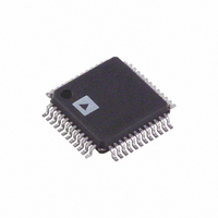
AD9763AST Analog Devices Inc, AD9763AST Datasheet - Page 24

AD9763AST
Manufacturer Part Number
AD9763AST
Description
IC DAC 10BIT DUAL 125MSPS 48LQFP
Manufacturer
Analog Devices Inc
Series
TxDAC+®r
Datasheet
1.AD9763ASTZ.pdf
(44 pages)
Specifications of AD9763AST
Rohs Status
RoHS non-compliant
Settling Time
35ns
Number Of Bits
10
Data Interface
Parallel
Number Of Converters
2
Voltage Supply Source
Analog and Digital
Power Dissipation (max)
450mW
Operating Temperature
-40°C ~ 85°C
Mounting Type
Surface Mount
Package / Case
48-LQFP
For Use With
AD9763-EBZ - BOARD EVAL FOR AD9763
Available stocks
Company
Part Number
Manufacturer
Quantity
Price
Company:
Part Number:
AD9763AST
Manufacturer:
AD
Quantity:
1 831
Company:
Part Number:
AD9763AST
Manufacturer:
ALTERA
Quantity:
591
Company:
Part Number:
AD9763ASTZ
Manufacturer:
ADI
Quantity:
180
Company:
Part Number:
AD9763ASTZ
Manufacturer:
Analog Devices Inc
Quantity:
10 000
Part Number:
AD9763ASTZ
Manufacturer:
ADI/亚德诺
Quantity:
20 000
Company:
Part Number:
AD9763ASTZRL
Manufacturer:
Analog Devices Inc
Quantity:
10 000
Part Number:
AD9763ASTZRL
Manufacturer:
ADI/亚德诺
Quantity:
20 000
AD9763/AD9765/AD9767
I
compliance range that must be adhered to in order to achieve
optimum performance. The negative output compliance range
of −1.0 V is set by the breakdown limits of the CMOS process.
Operation beyond this maximum limit may result in a breakdown
of the output stage and affect the reliability of the
AD9763/AD9765/AD9767.
The positive output compliance range is slightly dependent on
the full-scale output current, I
from 20 mA to 2 mA, the positive output compliance range
degrades slightly from its nominal 1.25 V to 1.00 V. The optimum
distortion performance for a single-ended or differential output
is achieved when the maximum full-scale signal at I
does not exceed 0.5 V. Applications requiring the AD9763/
AD9765/AD9767 output (that is, V
output compliance range must size R
beyond this compliance range adversely affects the linearity
performance of the AD9763/AD9765/AD9767 and
subsequently degrades its distortion performance.
DIGITAL INPUTS
The digital inputs of the AD9763/AD9765/AD9767 consist of
two independent channels. For the dual-port mode, each DAC has
its own dedicated 10-/12-/14-bit data port: WRT line and CLK line.
In the interleaved timing mode, the function of the digital control
pins changes as described in the Interleaved Mode Timing section.
The 10-/12-/14-bit parallel data inputs follow straight binary
coding, where the most significant bits (MSBs) are DB9P1 and
DB9P2 for the AD9763, DB11P1 and DB11P2 for the AD9765, and
DB13P1 and DB13P2 for the AD9767, and the least significant bits
(LSBs) are DB0P1 and DB0P2 for all three parts. I
full-scale output current when all data bits are at Logic 1. I
produces a complementary output with the full-scale current
split between the two outputs as a function of the input code.
The digital interface is implemented using an edge-triggered
master/slave latch. The DAC outputs are updated following
either the rising edge or every other rising edge of the clock,
depending on whether dual or interleaved mode is used. The
DAC outputs are designed to support a clock rate as high as
125 MSPS. The clock can be operated at any duty cycle that
meets the specified latch pulse width. The setup and hold times
can also be varied within the clock cycle as long as the specified
minimum times are met, although the location of these transition
edges may affect digital feedthrough and distortion performance.
Best performance is typically achieved when the input data
transitions on the falling edge of a 50% duty cycle clock.
DAC TIMING
The AD9763/AD9765/AD9767 can operate in two timing
modes, dual and interleaved, which are described in the
following sections. The block diagram in Figure 61 represents
the latch architecture in the interleaved timing mode.
OUTA
and I
OUTB
also have a negative and positive voltage
OUTFS
OUTA
. When I
LOAD
and/or V
accordingly. Operation
OUTFS
OUTB
OUTA
is decreased
OUTA
) to extend its
produces a
and I
OUTB
OUTB
Rev. F | Page 24 of 44
Dual-Port Mode Timing
When the MODE pin is at Logic 1, the AD9763/AD9765/AD9767
operates in dual-port mode (refer to Figure 57). The AD9763/
AD9765/AD9767 functions as two distinct DACs. Each DAC
has its own completely independent digital input and control lines.
The AD9763/AD9765/AD9767 features a double-buffered data
path. Data enters the device through the channel input latches.
This data is then transferred to the DAC latch in each signal
path. After the data is loaded into the DAC latch, the analog
output settles to its new value.
For general consideration, the WRT lines control the channel
input latches, and the CLK lines control the DAC latches. Both
sets of latches are updated on the rising edge of their respective
control signals.
The rising edge of CLK must occur before or simultaneously
with the rising edge of WRT. If the rising edge of CLK occurs
after the rising edge of WRT, a minimum delay of 2 ns must be
maintained from the rising edge of WRT to the rising edge of CLK.
Timing specifications for dual-port mode are shown in Figure 62
and Figure 63.
IQWRT
IQSEL
DATA IN, PORT 1
WRT1/WRT2
CLK1/CLK2
WRT1/WRT2
INTERLEAVED
CLK1/CLK2
DATA IN
DATA IN
I
I
OUTA
OUTB
IQRESET
I
I
OUTA
OUTB
OR
IQCLK
OR
Figure 61. Latch Structure in Interleaved Mode
D1
Figure 62. Dual-Port Mode Timing
Figure 63. Dual-Port Mode Timing
XX
D2
PORT 1
PORT 2
LATCH
LATCH
INPUT
INPUT
÷2
t
S
D1
D3
DAC1
LATCH
DAC2
LATCH
t
PD
D2
D4
DAC1
DAC2
t
H
t
t
LPW
CPW
DEINTERLEAVED
DATA OUT
D3
D5
D4


