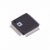
AD9763AST Analog Devices Inc, AD9763AST Datasheet - Page 30

AD9763AST
Manufacturer Part Number
AD9763AST
Description
IC DAC 10BIT DUAL 125MSPS 48LQFP
Manufacturer
Analog Devices Inc
Series
TxDAC+®r
Datasheet
1.AD9763ASTZ.pdf
(44 pages)
Specifications of AD9763AST
Rohs Status
RoHS non-compliant
Settling Time
35ns
Number Of Bits
10
Data Interface
Parallel
Number Of Converters
2
Voltage Supply Source
Analog and Digital
Power Dissipation (max)
450mW
Operating Temperature
-40°C ~ 85°C
Mounting Type
Surface Mount
Package / Case
48-LQFP
For Use With
AD9763-EBZ - BOARD EVAL FOR AD9763
Available stocks
Company
Part Number
Manufacturer
Quantity
Price
Company:
Part Number:
AD9763AST
Manufacturer:
AD
Quantity:
1 831
Company:
Part Number:
AD9763AST
Manufacturer:
ALTERA
Quantity:
591
Company:
Part Number:
AD9763ASTZ
Manufacturer:
ADI
Quantity:
180
Company:
Part Number:
AD9763ASTZ
Manufacturer:
Analog Devices Inc
Quantity:
10 000
Part Number:
AD9763ASTZ
Manufacturer:
ADI/亚德诺
Quantity:
20 000
Company:
Part Number:
AD9763ASTZRL
Manufacturer:
Analog Devices Inc
Quantity:
10 000
Part Number:
AD9763ASTZRL
Manufacturer:
ADI/亚德诺
Quantity:
20 000
AD9763/AD9765/AD9767
Note that the data in Figure 77 is given in terms of current out
vs. voltage in. Noise on the analog power supply has the effect
of modulating the internal current sources and therefore the
output current. The voltage noise on AVDD, therefore, is added
in a nonlinear manner to the desired I
dependent, thus producing mixing effects that can modulate
low frequency power supply noise to higher frequencies. Worst-
case PSRR for either one of the differential DAC outputs occurs
when the full-scale current is directed toward that output. As a
result, the PSRR measurement in Figure 77 represents a worst-
case condition in which the digital inputs remain static and the
full-scale output current of 20 mA is directed to the DAC
output being measured.
An example serves to illustrate the effect of supply noise on the
analog supply. Suppose a switching regulator with a switching
frequency of 250 kHz produces 10 mV of noise and, for simplicity’s
sake, all of this noise is concentrated at 250 kHz (that is, ignore
harmonics). To calculate how much of this undesired noise will
appear as current noise superimposed on the DAC full-scale
current, I
Figure 77 at 250 kHz. To calculate the PSRR for a given R
such that the units of PSRR are converted from A/V to V/V,
adjust the curve in Figure 77 by the scaling factor 20 × log(R
For example, if R
is, the PSRR of the DAC at 250 kHz, which is 85 dB in Figure 77,
becomes 51 dB V
OUTFS
, one must determine the PSRR in decibels using
OUT
LOAD
/V
is 50 Ω, the PSRR is reduced by 34 dB (that
IN
).
OUT
. PSRR is very code
LOAD
LOAD
Rev. F | Page 30 of 44
).
,
Proper grounding and decoupling are primary objectives in any
high speed, high resolution system. The AD9763/AD9765/AD9767
features separate analog and digital supply and ground pins to
optimize the management of analog and digital ground currents
in a system. In general, decouple the analog supply (AVDD) to
the analog common (ACOM) as close to the chip as physically
possible. Similarly, decouple the digital supply (DVDD1/DVDD2)
to the digital common (DCOM1/DCOM2) as close to the chip
as possible.
For those applications that require a single 5 V or 3.3 V supply
for both the analog and digital supplies, a clean analog supply
can be generated using the circuit shown in Figure 78. The
circuit consists of a differential LC filter with separate power
supply and return lines. Lower noise can be attained by using
low-ESR type electrolytic and tantalum capacitors.
TTL/CMOS
CIRCUITS
LOGIC
Figure 78. Differential LC Filter for Single 5 V and 3.3 V Applications
POWER SUPPLY
5V
FERRITE
BEADS
ELECTROLYTIC
100µF
TANTALUM
10µF
TO
22µF
CERAMIC
0.1µF
AVDD
ACOM


