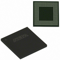
EPM570ZM256C6N Altera, EPM570ZM256C6N Datasheet - Page 53

EPM570ZM256C6N
Manufacturer Part Number
EPM570ZM256C6N
Description
IC MAX IIZ CPLD 570 LE 256-MBGA
Manufacturer
Altera
Series
MAX® IIr
Specifications of EPM570ZM256C6N
Programmable Type
In System Programmable
Delay Time Tpd(1) Max
9.0ns
Voltage Supply - Internal
1.71 V ~ 1.89 V
Number Of Logic Elements/blocks
570
Number Of Macrocells
440
Number Of I /o
160
Operating Temperature
0°C ~ 85°C
Mounting Type
Surface Mount
Package / Case
256-MBGA
Voltage
1.8V
Memory Type
FLASH
Number Of Logic Elements/cells
570
Lead Free Status / RoHS Status
Lead free / RoHS Compliant
Features
-
Other names
544-2453
Available stocks
Company
Part Number
Manufacturer
Quantity
Price
Company:
Part Number:
EPM570ZM256C6N
Manufacturer:
ALTERA
Quantity:
736
Chapter 4: Hot Socketing and Power-On Reset in MAX II Devices
Hot Socketing Feature Implementation in MAX II Devices
Figure 4–1. Hot Socketing Circuit Block Diagram for MAX II Devices
© October 2008 Altera Corporation
f
1
Make sure that the V
SRAM download has completed.
Each I/O and clock pin has the circuitry shown in
The POR circuit monitors V
until the device has completed its flash memory configuration of the SRAM logic. The
weak pull-up resistor (R) from the I/O pin to V
keep the I/O pins from floating. The 3.3-V tolerance control circuit permits the I/O
pins to be driven by 3.3 V before V
I/O pins from driving out when the device is not fully powered or operational. The
hot socket circuit prevents I/O pins from internally powering V
driven by external signals before the device is powered.
For information about 5.0-V tolerance, refer to the
Voltage Systems
Figure 4–2
This design ensures that the output buffers do not drive when V
V
voltage spikes during hot insertion. The V
tolerant circuit capacitance.
Resistor
Pull-Up
CCINT
Weak
PAD
or if the I/O pad voltage is higher than V
shows a transistor-level cross section of the MAX II device I/O buffers.
chapter in the MAX II Device Handbook.
V
CCINT
CCIO
is within the recommended operating range even though
CCINT
and V
Input Buffer
to Logic Array
CCIO
Tolerance
Voltage
Control
CCIO
and/or V
voltage levels and keeps I/O pins tri-stated
PAD
Output Enable
leakage current charges the 3.3-V
CCIO
CCIO
CCINT
Using MAX II Devices in Multi-
Figure
. This also applies for sudden
is enabled during download to
Hot Socket
are powered, and it prevents the
Power On
Monitor
Reset
4–1.
CCIO
CCIO
is powered before
and V
MAX II Device Handbook
CCINT
when
4–3


