DSPB56362AG120 Freescale Semiconductor, DSPB56362AG120 Datasheet - Page 59
DSPB56362AG120
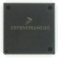
Manufacturer Part Number
DSPB56362AG120
Description
IC DSP 24BIT AUD 120MHZ 144-LQFP
Manufacturer
Freescale Semiconductor
Series
Symphony™r
Type
Audio Processorr
Datasheet
1.DSPB56362AG120.pdf
(152 pages)
Specifications of DSPB56362AG120
Interface
Host Interface, I²C, SAI, SPI
Clock Rate
120MHz
Non-volatile Memory
ROM (126 kB)
On-chip Ram
42kB
Voltage - I/o
3.30V
Voltage - Core
3.30V
Operating Temperature
-40°C ~ 85°C
Mounting Type
Surface Mount
Package / Case
144-LQFP
Device Core Size
24b
Architecture
Modified Harvard
Format
Fixed Point
Clock Freq (max)
120MHz
Mips
120
Device Input Clock Speed
120MHz
Ram Size
42KB
Program Memory Size
90KB
Operating Supply Voltage (typ)
3.3V
Operating Supply Voltage (min)
3.14V
Operating Supply Voltage (max)
3.46V
Operating Temp Range
-40C to 105C
Operating Temperature Classification
Industrial
Mounting
Surface Mount
Pin Count
144
Package Type
LQFP
Product
DSPs
Data Bus Width
24 bit
Processor Series
DSP563xx
Core
56000
Numeric And Arithmetic Format
Fixed-Point
Instruction Set Architecture
Modified Harvard
Device Million Instructions Per Second
120 MIPS
Maximum Clock Frequency
120 MHz
Program Memory Type
Flash
Data Ram Size
42 KB
Operating Supply Voltage
3.3 V
Maximum Operating Temperature
+ 105 C
Mounting Style
SMD/SMT
Interface Type
SPI, I2C, ESAI, SHI
Minimum Operating Temperature
- 40 C
Lead Free Status / RoHS Status
Lead free / RoHS Compliant
Available stocks
Company
Part Number
Manufacturer
Quantity
Price
Company:

Part Number:
DSPB56362AG120
Manufacturer:
FSC
Quantity:
12 000
Company:
Part Number:
DSPB56362AG120
Manufacturer:
FREESCA
Quantity:
273
Company:
Part Number:
DSPB56362AG120
Manufacturer:
Freescale Semiconductor
Quantity:
10 000
Part Number:
DSPB56362AG120
Manufacturer:
N/A
Quantity:
20 000


Freescale Semiconductor
1
2
3
4
5
No.
157
158
159
160
182
183
184
185
186
187
188
189
190
191
192
193
194
195
No.
The number of wait states for out-of-page access is specified in the DCR.
The refresh period is specified in the DCR.
RD deassertion will always occur after CAS deassertion; therefore, the restricted timing is t
The asynchronous delays specified in the expressions are valid for DSP56362.
Either t
Table 3-16 DRAM Out-of-Page and Refresh Timings, Fifteen Wait States 100 and 120MHz
Random read or write cycle time
RAS assertion to data valid (read)
CAS assertion to data valid (read)
Column address valid to data valid (read)
WR assertion pulse width
WR assertion to RAS deassertion
WR assertion to CAS deassertion
Data valid to CAS assertion (write)
CAS assertion to data not valid (write)
RAS assertion to data not valid (write)
WR assertion to CAS assertion
CAS assertion to RAS assertion (refresh)
RAS deassertion to CAS assertion (refresh)
RD assertion to RAS deassertion
RD assertion to data valid
RD deassertion to data not valid
WR assertion to data active
WR deassertion to data high impedance
Table 3-15 DRAM Out-of-Page and Refresh Timings, Eleven Wait States
RCH
or t
RRH
Characteristics
must be satisfied for read cycles.
Characteristics
3
3
DSP56362 Technical Data, Rev. 4
3
Symbol
t
t
t
RAC
CAC
t
RC
AA
8.25 × T
4.75 × T
5.5 × T
Expression
16 × T
Symbol
t
t
t
t
t
t
t
t
RWL
CWL
WCS
ROH
t
t
DHR
CSR
RPC
t
t
WP
DS
DH
GA
GZ
C
C
C
− 5.7
C
− 5.7
− 5.7
11.75 × T
10.25 × T
External Memory Expansion Port (Port A)
11.5 × T
5.75 × T
5.25 × T
7.75 × T
2.75 × T
11.5 × T
0.75 × T
6.5 × T
1.5 × T
Expression
10 × T
160.0
0.25 × T
Min
—
—
—
100 MHz
C
C
C
C
C
C
C
C
C
C
C
C
− 7.0
− 4.3
− 4.0
− 4.5
− 4.0
− 4.0
− 4.0
− 4.0
− 4.0
− 0.3
− 4.3
− 4.3
C
Max
76.8
41.8
49.3
OFF
—
4
1, 2
and not t
110.5
113.2
103.2
111.0
(continued)
53.5
48.5
73.5
60.7
11.0
23.5
Min
133.3
0.0
7.2
—
Min
100 MHz
—
—
120 MHz
GZ
.
Max
93.0
2.5
Max
—
—
—
—
—
—
—
—
—
—
—
—
63.0
33.9
40.1
—
1, 2
Unit
Unit
ns
ns
ns
ns
ns
ns
ns
ns
ns
ns
ns
ns
ns
ns
ns
ns
ns
ns
3-33
Related parts for DSPB56362AG120
Image
Part Number
Description
Manufacturer
Datasheet
Request
R

Part Number:
Description:
Manufacturer:
Freescale Semiconductor, Inc
Datasheet:
Part Number:
Description:
Manufacturer:
Freescale Semiconductor, Inc
Datasheet:
Part Number:
Description:
Manufacturer:
Freescale Semiconductor, Inc
Datasheet:
Part Number:
Description:
Manufacturer:
Freescale Semiconductor, Inc
Datasheet:
Part Number:
Description:
Manufacturer:
Freescale Semiconductor, Inc
Datasheet:
Part Number:
Description:
Manufacturer:
Freescale Semiconductor, Inc
Datasheet:
Part Number:
Description:
Manufacturer:
Freescale Semiconductor, Inc
Datasheet:
Part Number:
Description:
Manufacturer:
Freescale Semiconductor, Inc
Datasheet:
Part Number:
Description:
Manufacturer:
Freescale Semiconductor, Inc
Datasheet:
Part Number:
Description:
Manufacturer:
Freescale Semiconductor, Inc
Datasheet:
Part Number:
Description:
Manufacturer:
Freescale Semiconductor, Inc
Datasheet:
Part Number:
Description:
Manufacturer:
Freescale Semiconductor, Inc
Datasheet:
Part Number:
Description:
Manufacturer:
Freescale Semiconductor, Inc
Datasheet:
Part Number:
Description:
Manufacturer:
Freescale Semiconductor, Inc
Datasheet:
Part Number:
Description:
Manufacturer:
Freescale Semiconductor, Inc
Datasheet: