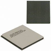
EP1AGX90EF1152I6N Altera, EP1AGX90EF1152I6N Datasheet - Page 77

EP1AGX90EF1152I6N
Manufacturer Part Number
EP1AGX90EF1152I6N
Description
IC ARRIA GX FPGA 90K 1152FBGA
Manufacturer
Altera
Series
Arria GXr
Datasheet
1.EP1AGX20CF484C6N.pdf
(234 pages)
Specifications of EP1AGX90EF1152I6N
Number Of Logic Elements/cells
90220
Number Of Labs/clbs
4511
Total Ram Bits
4477824
Number Of I /o
538
Voltage - Supply
1.15 V ~ 1.25 V
Mounting Type
Surface Mount
Operating Temperature
-40°C ~ 100°C
Package / Case
1152-FBGA
Lead Free Status / RoHS Status
Lead free / RoHS Compliant
Number Of Gates
-
Other names
544-2387
Available stocks
Company
Part Number
Manufacturer
Quantity
Price
- Current page: 77 of 234
- Download datasheet (4Mb)
Chapter 2: Arria GX Architecture
PLLs and Clock Networks
Figure 2–60. External PLL Output Clock Control Blocks
Notes to
(1) These clock select signals can only be set through a configuration file (.sof or .pof) and cannot be dynamically controlled during user mode
(2) The clock control block feeds to a multiplexer within the PLL_OUT pin’s IOE. The PLL_OUT pin is a dual-purpose pin. Therefore, this multiplexer
© December 2009 Altera Corporation
operation.
selects either an internal signal or the output of the clock control block.
Figure
2–60:
For the global clock control block, clock source selection can be controlled either
statically or dynamically. You have the option of statically selecting the clock source
by using the Quartus II software to set specific configuration bits in the configuration
file (.sof or .pof) or controlling the selection dynamically by using internal logic to
drive the multiplexer select inputs. When selecting statically, the clock source can be
set to any of the inputs to the select multiplexer. When selecting the clock source
dynamically, you can either select between two PLL outputs (such as the C0 or C1
outputs from one PLL), between two PLLs (such as the C0/C1 clock output of one
PLL or the C0/C1 c1ock output of the other PLL), between two clock pins (such as
CLK0 or CLK1), or between a combination of clock pins or PLL outputs.
For the regional and PLL_OUT clock control block, clock source selection can only be
controlled statically using configuration bits. Any of the inputs to the clock select
multiplexer can be set as the clock source.
Arria GX clock networks can be disabled (powered down) by both static and dynamic
approaches. When a clock net is powered down, all logic fed by the clock net is in an
off-state thereby reducing the overall power consumption of the device. GCLK and
RCLK networks can be powered down statically through a setting in the
configuration file (.sof or .pof). Clock networks that are not used are automatically
powered down through configuration bit settings in the configuration file generated
by the Quartus II software. The dynamic clock enable or disable feature allows the
internal logic to control power up/down synchronously on GCLK and RCLK nets and
PLL_OUT pins. This function is independent of the PLL and is applied directly on the
clock network or PLL_OUT pin, as shown in
IOE
Internal
Logic
(2)
Outputs (c[5..0])
PLL Counter
PLL_OUT
Enable/
Disable
Pin
6
Internal
Static Clock
Select (1)
Logic
Static Clock Select
Figure 2–58
(1)
through
Arria GX Device Handbook, Volume 1
Figure
2–60.
2–71
Related parts for EP1AGX90EF1152I6N
Image
Part Number
Description
Manufacturer
Datasheet
Request
R

Part Number:
Description:
CYCLONE II STARTER KIT EP2C20N
Manufacturer:
Altera
Datasheet:

Part Number:
Description:
CPLD, EP610 Family, ECMOS Process, 300 Gates, 16 Macro Cells, 16 Reg., 16 User I/Os, 5V Supply, 35 Speed Grade, 24DIP
Manufacturer:
Altera Corporation
Datasheet:

Part Number:
Description:
CPLD, EP610 Family, ECMOS Process, 300 Gates, 16 Macro Cells, 16 Reg., 16 User I/Os, 5V Supply, 15 Speed Grade, 24DIP
Manufacturer:
Altera Corporation
Datasheet:

Part Number:
Description:
Manufacturer:
Altera Corporation
Datasheet:

Part Number:
Description:
CPLD, EP610 Family, ECMOS Process, 300 Gates, 16 Macro Cells, 16 Reg., 16 User I/Os, 5V Supply, 30 Speed Grade, 24DIP
Manufacturer:
Altera Corporation
Datasheet:

Part Number:
Description:
High-performance, low-power erasable programmable logic devices with 8 macrocells, 10ns
Manufacturer:
Altera Corporation
Datasheet:

Part Number:
Description:
High-performance, low-power erasable programmable logic devices with 8 macrocells, 7ns
Manufacturer:
Altera Corporation
Datasheet:

Part Number:
Description:
Classic EPLD
Manufacturer:
Altera Corporation
Datasheet:

Part Number:
Description:
High-performance, low-power erasable programmable logic devices with 8 macrocells, 10ns
Manufacturer:
Altera Corporation
Datasheet:

Part Number:
Description:
Manufacturer:
Altera Corporation
Datasheet:

Part Number:
Description:
Manufacturer:
Altera Corporation
Datasheet:

Part Number:
Description:
Manufacturer:
Altera Corporation
Datasheet:

Part Number:
Description:
CPLD, EP610 Family, ECMOS Process, 300 Gates, 16 Macro Cells, 16 Reg., 16 User I/Os, 5V Supply, 25 Speed Grade, 24DIP
Manufacturer:
Altera Corporation
Datasheet:


