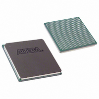
EP1S10F780I6N Altera, EP1S10F780I6N Datasheet - Page 452

EP1S10F780I6N
Manufacturer Part Number
EP1S10F780I6N
Description
IC STRATIX FPGA 10K LE 780-FBGA
Manufacturer
Altera
Series
Stratix®r
Datasheet
1.EP1S10F484I6N.pdf
(864 pages)
Specifications of EP1S10F780I6N
Number Of Logic Elements/cells
10570
Number Of Labs/clbs
1057
Total Ram Bits
920448
Number Of I /o
426
Voltage - Supply
1.425 V ~ 1.575 V
Mounting Type
Surface Mount
Operating Temperature
0°C ~ 85°C
Package / Case
780-FBGA
Lead Free Status / RoHS Status
Lead free / RoHS Compliant
Number Of Gates
-
Available stocks
Company
Part Number
Manufacturer
Quantity
Price
Company:
Part Number:
EP1S10F780I6N
Manufacturer:
ALTERA
Quantity:
3 000
- Current page: 452 of 864
- Download datasheet (11Mb)
Stratix & Stratix GX I/O Banks
4–24
Stratix Device Handbook, Volume 2
Non-Voltage-Referenced Standards
Each Stratix I/O bank has its own VCCIO pins and supports only one
V
support any number of input signals with different I/O standard
assignments, as shown in
For output signals, a single I/O bank can only support non-voltage-
referenced output signals driving at the same voltage as V
I/O bank can only have one V
value for non-voltage referenced signals. For example, an I/O bank with
a 2.5-V V
HyperTransport technology inputs and outputs, and 3.3-V LVCMOS
inputs (not output or bidirectional pins).
1
Voltage-Referenced Standards
To accommodate voltage-referenced I/O standards, each Stratix I/O
bank supports multiple VREF pins feeding a common VREF bus. The
number of available VREF pins increases as device density increases. If
these pins are not used as VREF pins, they can not be used as generic I/O
pins.
Notes to
(1)
(2)
3.3 V
2.5 V
1.8 V
1.5 V
Table 4–5. Acceptable Input Levels for LVTTL/LVCMOS
CCIO
Bank V
Because the input signal will not drive to the rail, the input buffer does not
completely shut off, and the I/O current will be slightly higher than the default
value.
These input values overdrive the input buffer, so the pin leakage current will be
slightly higher than the default value.
, either 1.5, 1.8, 2.5 or 3.3 V. A Stratix I/O bank can simultaneously
Table
If the output buffer overdrives the input buffer, you must turn
on the Allow voltage overdrive for LVTTL/LVCMOS option in
the Quartus II software. To see this option, click the Device &
Pin Options button in the Device page of the Settings dialog
box (Assignments menu). Then click the Pin Placement tab in
the Device & Pin Options dialog box.
CCIO
CCIO
setting can support 2.5-V LVTTL inputs and outputs,
4–5:
v
v
3.3 V
v
v
(2)
(2)
Table
CCIO
4–5.
Acceptable Input Levels
v
v
2.5 V
value, so it can only drive out that one
v
v
(2)
(2)
1.8 V
v
v
Altera Corporation
CCIO
. A Stratix
June 2006
v
1.5 V
v
(1)
Related parts for EP1S10F780I6N
Image
Part Number
Description
Manufacturer
Datasheet
Request
R

Part Number:
Description:
CYCLONE II STARTER KIT EP2C20N
Manufacturer:
Altera
Datasheet:

Part Number:
Description:
CPLD, EP610 Family, ECMOS Process, 300 Gates, 16 Macro Cells, 16 Reg., 16 User I/Os, 5V Supply, 35 Speed Grade, 24DIP
Manufacturer:
Altera Corporation
Datasheet:

Part Number:
Description:
CPLD, EP610 Family, ECMOS Process, 300 Gates, 16 Macro Cells, 16 Reg., 16 User I/Os, 5V Supply, 15 Speed Grade, 24DIP
Manufacturer:
Altera Corporation
Datasheet:

Part Number:
Description:
Manufacturer:
Altera Corporation
Datasheet:

Part Number:
Description:
CPLD, EP610 Family, ECMOS Process, 300 Gates, 16 Macro Cells, 16 Reg., 16 User I/Os, 5V Supply, 30 Speed Grade, 24DIP
Manufacturer:
Altera Corporation
Datasheet:

Part Number:
Description:
High-performance, low-power erasable programmable logic devices with 8 macrocells, 10ns
Manufacturer:
Altera Corporation
Datasheet:

Part Number:
Description:
High-performance, low-power erasable programmable logic devices with 8 macrocells, 7ns
Manufacturer:
Altera Corporation
Datasheet:

Part Number:
Description:
Classic EPLD
Manufacturer:
Altera Corporation
Datasheet:

Part Number:
Description:
High-performance, low-power erasable programmable logic devices with 8 macrocells, 10ns
Manufacturer:
Altera Corporation
Datasheet:

Part Number:
Description:
Manufacturer:
Altera Corporation
Datasheet:

Part Number:
Description:
Manufacturer:
Altera Corporation
Datasheet:

Part Number:
Description:
Manufacturer:
Altera Corporation
Datasheet:

Part Number:
Description:
CPLD, EP610 Family, ECMOS Process, 300 Gates, 16 Macro Cells, 16 Reg., 16 User I/Os, 5V Supply, 25 Speed Grade, 24DIP
Manufacturer:
Altera Corporation
Datasheet:


