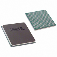
EP1S10F780I6N Altera, EP1S10F780I6N Datasheet - Page 546

EP1S10F780I6N
Manufacturer Part Number
EP1S10F780I6N
Description
IC STRATIX FPGA 10K LE 780-FBGA
Manufacturer
Altera
Series
Stratix®r
Datasheet
1.EP1S10F484I6N.pdf
(864 pages)
Specifications of EP1S10F780I6N
Number Of Logic Elements/cells
10570
Number Of Labs/clbs
1057
Total Ram Bits
920448
Number Of I /o
426
Voltage - Supply
1.425 V ~ 1.575 V
Mounting Type
Surface Mount
Operating Temperature
0°C ~ 85°C
Package / Case
780-FBGA
Lead Free Status / RoHS Status
Lead free / RoHS Compliant
Number Of Gates
-
Available stocks
Company
Part Number
Manufacturer
Quantity
Price
Company:
Part Number:
EP1S10F780I6N
Manufacturer:
ALTERA
Quantity:
3 000
- Current page: 546 of 864
- Download datasheet (11Mb)
Software Support
Figure 5–47. SERDES Bypass LVDS Receiver with Logic Array as Deserializer
5–74
Stratix Device Handbook, Volume 2
data in
Serial
Clock
×4 clock0
÷2 clock1
PLL
Logic Array as Serializer/Deserializer Interface
The design can use the lpm_shift_reg megafunction instead of a
simple dual port memory block to serialize/deserialize data. The receiver
requires an extra flip-flop clocked by the slow clock to latch on to the
deserialized data. The transmitter requires a counter to generate the
enable signal for the shift register to indicate the times to load and
serialize the data.
LVDS receiver and
array performing the deserialization.
This scheme can also be used for APEX II and Mercury device flexible
LVDS solutions.
Input
DDR
data_h
data_l
Figures 5–47
clock
data
data
clock
×
8 LVDS transmitter, respectively, with the logic
Register
Register
data[1, 3, 5, 7]
data[0, 2, 4, 6]
Shift
Shift
and
5–48
data[7..0]
show the schematic of the
D
CLK
DFF[7..0]
Altera Corporation
Q
July 2005
Data to
logic array
rx_clk
×
8
Related parts for EP1S10F780I6N
Image
Part Number
Description
Manufacturer
Datasheet
Request
R

Part Number:
Description:
CYCLONE II STARTER KIT EP2C20N
Manufacturer:
Altera
Datasheet:

Part Number:
Description:
CPLD, EP610 Family, ECMOS Process, 300 Gates, 16 Macro Cells, 16 Reg., 16 User I/Os, 5V Supply, 35 Speed Grade, 24DIP
Manufacturer:
Altera Corporation
Datasheet:

Part Number:
Description:
CPLD, EP610 Family, ECMOS Process, 300 Gates, 16 Macro Cells, 16 Reg., 16 User I/Os, 5V Supply, 15 Speed Grade, 24DIP
Manufacturer:
Altera Corporation
Datasheet:

Part Number:
Description:
Manufacturer:
Altera Corporation
Datasheet:

Part Number:
Description:
CPLD, EP610 Family, ECMOS Process, 300 Gates, 16 Macro Cells, 16 Reg., 16 User I/Os, 5V Supply, 30 Speed Grade, 24DIP
Manufacturer:
Altera Corporation
Datasheet:

Part Number:
Description:
High-performance, low-power erasable programmable logic devices with 8 macrocells, 10ns
Manufacturer:
Altera Corporation
Datasheet:

Part Number:
Description:
High-performance, low-power erasable programmable logic devices with 8 macrocells, 7ns
Manufacturer:
Altera Corporation
Datasheet:

Part Number:
Description:
Classic EPLD
Manufacturer:
Altera Corporation
Datasheet:

Part Number:
Description:
High-performance, low-power erasable programmable logic devices with 8 macrocells, 10ns
Manufacturer:
Altera Corporation
Datasheet:

Part Number:
Description:
Manufacturer:
Altera Corporation
Datasheet:

Part Number:
Description:
Manufacturer:
Altera Corporation
Datasheet:

Part Number:
Description:
Manufacturer:
Altera Corporation
Datasheet:

Part Number:
Description:
CPLD, EP610 Family, ECMOS Process, 300 Gates, 16 Macro Cells, 16 Reg., 16 User I/Os, 5V Supply, 25 Speed Grade, 24DIP
Manufacturer:
Altera Corporation
Datasheet:


