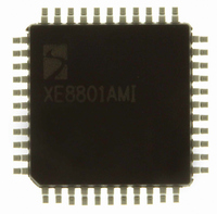
XE8801AMI027LF Semtech, XE8801AMI027LF Datasheet - Page 96

XE8801AMI027LF
Manufacturer Part Number
XE8801AMI027LF
Description
IC DAS 16BIT FLASH 8K MTP 44LQFP
Manufacturer
Semtech
Datasheet
1.XE8801AMI027LF.pdf
(135 pages)
Specifications of XE8801AMI027LF
Applications
Sensing Machine
Core Processor
RISC
Program Memory Type
FLASH (22 kB)
Controller Series
XE8000
Ram Size
512 x 8
Interface
UART, USRT
Number Of I /o
24
Voltage - Supply
2.4 V ~ 5.5 V
Operating Temperature
-40°C ~ 85°C
Mounting Type
Surface Mount
Package / Case
44-LQFP
For Use With
XE8000MP - PROG BOARD AND PROSTART2 CARD
Lead Free Status / RoHS Status
Lead free / RoHS Compliant
Available stocks
Company
Part Number
Manufacturer
Quantity
Price
- Current page: 96 of 135
- Download datasheet (2Mb)
16.6.3
The second PGA has a finer gain and offset tuning capability, as shown in Table 16-15 and Table 16-16. The voltage
V
where GD
PGA2_GAIN[1:0] and PGA2_OFFSET[3:0].
As shown in equation 6, the offset correction is directly proportional to the reference voltage. All drifts and
perturbations on the reference voltage will affect the precision of the offset compensation.
16.6.4
The finest gain and offset tuning is performed with the third and last PGA stage, according to the coding of Table
16-17 and Table 16-18. The output of PGA3 is also the input of the ADC. Thus, similarly to PGA2, we find that the
voltage entering the ADC is given by:
where GD
PGA3_GAIN[6:0] and PGA3_OFFSET[6:0] . To remain within the signal compliance of the PGA stages, the
condition:
must be verified.
As shown in equation 7, the offset correction is directly proportional to the reference voltage. All drifts and
perturbations on the reference voltage will affect the precision of the offset compensation.
Finally, combining equations Eq. 5 to Eq. 7 for the three PGA stages, the input voltage V
to V
where the total PGA gain is defined as:
and the total PGA offset is:
© Semtech 2005
D2
at the output of PGA2 is given by:
IN
by:
V
V
V
V
GD
GDoff
D
IN
D
IN
2
1
2
PGA2
PGA3
,
3
,
,
TOT
ADC
ADC
and GDoff
V
=
and GDoff
D
GD
TOT
2
=
=
=
<
GD
GD
GD
2
=
V
⋅
GDoff
V
DD
3
3
TOT
D
⋅
⋅
1
V
GD
2
−
⋅
D
(V)
are respectively the gain and offset of PGA2 (in V/V). These are controlled with the words
V
GDoff
2
3
3
2
IN
−
+
⋅
are respectively the gain and offset of PGA3 (in V/V). The control words are
GD
GDoff
−
GD
GDoff
2
1
3
⋅
V
⋅
3
GDoff
REF
⋅
TOT
V
REF
⋅
V
2
(V)
(V/V)
REF
(V)
(V)
(V/V)
16-11
(Eq. 6)
(Eq. 7)
(Eq. 8)
(Eq. 9)
(Eq. 10)
(Eq. 11)
XE8801A – SX8801R
IN,ADC
of the ADC is related
www.semtech.com
Related parts for XE8801AMI027LF
Image
Part Number
Description
Manufacturer
Datasheet
Request
R

Part Number:
Description:
EVALUATION BOARD
Manufacturer:
Semtech
Datasheet:

Part Number:
Description:
EVALUATION BOARD
Manufacturer:
Semtech
Datasheet:

Part Number:
Description:
VOLTAGE SUPPRESSOR, TRANSIENT SEMTECH
Manufacturer:
Semtech
Datasheet:

Part Number:
Description:
HIGH VOLTAGE CAPACITORS MONOLITHIC CERAMIC TYPE
Manufacturer:
Semtech Corporation
Datasheet:

Part Number:
Description:
EZ1084CM5.0 AMP POSITIVE VOLTAGE REGULATOR
Manufacturer:
Semtech Corporation
Datasheet:

Part Number:
Description:
3.0 AMP LOW DROPOUT POSITIVE VOLTAGE REGULATORS
Manufacturer:
Semtech Corporation
Datasheet:

Part Number:
Description:
Manufacturer:
Semtech Corporation
Datasheet:

Part Number:
Description:
RailClamp Low Capacitance TVS Diode Array
Manufacturer:
Semtech Corporation
Datasheet:

Part Number:
Description:
Manufacturer:
Semtech Corporation
Datasheet:

Part Number:
Description:
Manufacturer:
Semtech Corporation
Datasheet:

Part Number:
Description:
Manufacturer:
Semtech Corporation
Datasheet:

Part Number:
Description:
Manufacturer:
Semtech Corporation
Datasheet:


