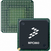
MPC8241LVR200D Freescale Semiconductor, MPC8241LVR200D Datasheet - Page 38

MPC8241LVR200D
Manufacturer Part Number
MPC8241LVR200D
Description
IC MPU 32BIT 200MHZ PPC 357-PBGA
Manufacturer
Freescale Semiconductor
Series
PowerPCr
Datasheet
1.MPC8241LZQ200D.pdf
(58 pages)
Specifications of MPC8241LVR200D
Processor Type
MPC82xx PowerQUICC II 32-bit
Speed
200MHz
Voltage
1.8V
Mounting Type
Surface Mount
Package / Case
357-PBGA
Processor Series
MPC8xxx
Core
603e
Maximum Clock Frequency
200 MHz
Maximum Operating Temperature
+ 105 C
Mounting Style
SMD/SMT
Minimum Operating Temperature
0 C
Core Size
32 Bit
Program Memory Size
32KB
Cpu Speed
200MHz
Digital Ic Case Style
BGA
No. Of Pins
357
Supply Voltage Range
1.14V To 1.26V
Operating Temperature Range
0°C To +105°C
Family Name
MPC82XX
Device Core
PowerQUICC II
Device Core Size
32b
Frequency (max)
200MHz
Instruction Set Architecture
RISC
Supply Voltage 1 (typ)
1.8V
Operating Supply Voltage (max)
1.9V
Operating Supply Voltage (min)
1.7V
Operating Temp Range
0C to 105C
Operating Temperature Classification
Commercial
Mounting
Surface Mount
Pin Count
357
Package Type
BGA
Rohs Compliant
Yes
Lead Free Status / RoHS Status
Lead free / RoHS Compliant
Features
-
Lead Free Status / Rohs Status
Lead free / RoHS Compliant
Available stocks
Company
Part Number
Manufacturer
Quantity
Price
Company:
Part Number:
MPC8241LVR200D
Manufacturer:
Freescale Semiconductor
Quantity:
135
Company:
Part Number:
MPC8241LVR200D
Manufacturer:
Freescale Semiconductor
Quantity:
10 000
Part Number:
MPC8241LVR200D
Manufacturer:
FREESCALE
Quantity:
20 000
Package Description
38
Notes:
1. Multi-pin signals such as AD[31:0] or MDL[0:31] physical package pin numbers are listed in order corresponding to the signal
2. This pin is affected by a programmable PCI_HOLD_DEL parameter.
3. A weak pull-up resistor (2–10 kΩ) should be placed on this PCI control pin to LV
4. GNT4 is a reset configuration pin with an internal pull-up resistor that is enabled only when in the reset state.
5. This pin is a multiplexed signal and appears more than once in this table.
6. This pin has an internal pull-up resistor that is enabled at all times. The value of the internal pull-up resistor is not guaranteed,
7. This pin is a sustained three-state pin as defined by the PCI Local Bus Specification (Rev. 2.2).
8. This pin is an open-drain signal.
9. DL[0] is a reset configuration pin with an internal pull-up resistor that is enabled only when in the reset state. The value of the
10.This pin has an internal pull-up resistor that is enabled only when in the reset state. The value of the internal pull-up resistor
11.This pin is a reset configuration pin.
12.A weak pull-up resistor (2–10 kΩ) should be placed on this pin to GV
13.V
14.External PCI clocking source or fanout buffer may be required for system if using the MPC8241 DUART functionality because
15.OSC_IN uses the 3.3-V PCI interface driver, which is 5-V tolerant. See
16.This pin can be programmed as driven (default) or as open-drain (in MIOCR 1).
17.All grounded pins are connected together. Connections should not be made to individual pins. The list represents the balls
18.GV
19.Treat these pins as no connects unless debug address functionality is used.
20.PLL_CFG signals must be driven on reset and must be held for at least 25 clock cycles after the negation of HRST_CTRL
21.Place a pull-up resistor of 120 Ω or less on the TEST0 pin.
22.SDRAM_CLK[0:3] and SDRAM_SYNC_OUT signals use DRV_MEM_CTRL for chip Rev. 1.1 (A). These signals use
23.The driver capability of this pin is hardwired to 40 Ω and cannot be changed.
24.Freescale typically expects that customers using the serial port will have sufficient drivers available in the RS232 transceiver
25. HRST_CPU/HRST_CTRL must transition from a logic 0 to a logic 1 in less than one SDRAM_SYNC_IN clock cycle for the
names. Ex: AD0 is on pin U1, AD1 is on pin U2,..., AD31 is on pin U13.
but is sufficient to prevent unused inputs from floating.
internal pull-up resistor is not guaranteed, but is sufficient to ensure that a logic 1 is read into configuration bits during reset.
is not guaranteed, but is sufficient to ensure that a logic 1 is read into configuration bits during reset.
PCI_CLK[0:3] are not available in DUART mode. Only PCI_CLK4 is available in DUART mode.
that are connected to ground.
GV
Connections should not be made to individual PWRRING pins.
and HRST_CPU in order to be latched.
DRV_MEM_CLK for chip Rev. 1.2B.
to drive the CTS pin actively as an input if they are using that mode. No pullups would be needed in these circumstances.
device to be in the nonreset state
IH
PLL_CFG[0:4]
Signal Name
DD
DD
and V
DA[12:13]
DA[14:15]
DA[10:6]/
_OV
DA[11]
_OV
IL
DD
DD
for these signals are the same as the PCI V
must not exceed V
pins are all shorted together, PWRRING. The list represents the balls that are connected to PWRRING.
N3 N2 N1 M4 M3
T13
M16 N16
B6 D8
MPC8241 Integrated Processor Hardware Specifications, Rev. 10
Package Pin Number
DD
Table 16. MPC8241 Pinout Listing (continued)
/AV
DD
/AV
DD
2 by more than 1.8 V at any time including during power-on reset. Note that
IH
and V
Pin Type
Output
Output
Output
I/O
IL
entries in
DD
Table 2
_OV
GV
GV
GV
GV
Supply
DD
Table
Power
DD
DD
DD
DD
.
for details.
_OV
_OV
_OV
_OV
DD
.
3.
DD
DD
DD
DD
DRV_MEM_CTRL
DRV_STD_MEM
Driver Type
DRV_PCI
Output
Freescale Semiconductor
—
1, 5, 20
Notes
1, 19
1, 19
19


