MC68EC030FE25C Freescale Semiconductor, MC68EC030FE25C Datasheet - Page 13
MC68EC030FE25C
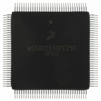
Manufacturer Part Number
MC68EC030FE25C
Description
IC MPU 32 BIT ENHANCED 132-CQFP
Manufacturer
Freescale Semiconductor
Specifications of MC68EC030FE25C
Processor Type
M680x0 32-Bit
Speed
25MHz
Voltage
5V
Mounting Type
Surface Mount
Package / Case
132-CQFP
Family Name
M68000
Device Core
ColdFire
Device Core Size
32b
Frequency (max)
25MHz
Instruction Set Architecture
RISC
Supply Voltage 1 (typ)
5V
Operating Supply Voltage (max)
5.25V
Operating Supply Voltage (min)
4.75V
Operating Temp Range
0C to 70C
Operating Temperature Classification
Commercial
Mounting
Surface Mount
Pin Count
132
Package Type
CQUAD
Lead Free Status / RoHS Status
Contains lead / RoHS non-compliant
Features
-
Lead Free Status / Rohs Status
Compliant
Available stocks
Company
Part Number
Manufacturer
Quantity
Price
Company:

Part Number:
MC68EC030FE25C
Manufacturer:
MOTOROLA
Quantity:
1
Company:
Part Number:
MC68EC030FE25C
Manufacturer:
MOTOROLA
Quantity:
325
Company:
Part Number:
MC68EC030FE25C
Manufacturer:
Freescale Semiconductor
Quantity:
10 000
Part Number:
MC68EC030FE25C
Manufacturer:
MOTOROLA/摩托罗拉
Quantity:
20 000
Company:
Part Number:
MC68EC030FE25CB1
Manufacturer:
Freescale Semiconductor
Quantity:
10 000


DATA CACHE
OPERAND TRANSFER MECHANISM
M O T O R O L A
The organization of the data cache (see Figure 7) is similar to that of the instruction cache. However, the
tag is composed of the upper 24 address bits, the four valid bits, and all three function code bits, explicitly
specifying the address space associated with each line. The data cache employs a write-through policy
with programmable write allocation of data writes— i.e., if a cache hit occurs on a write cycle, both the data
cache and the external device are updated with the new data. If a write cycle generates a cache miss, the
external device is updated, and a new data cache entry can be replaced or allocated for that address,
depending on the state of the write-allocate (WA) bit in the CACR.
The MC68EC030 offers three different mechanisms by which data can be transferred into and out of the
chip. Asynchronous bus cycles, compatible with the asynchronous bus on the MC68020 and MC68030,
can transfer data in a minimum of three clock cycles; the amount of data transferred on each cycle is
determined by the dynamic bus sizing mechanism on a cycle-by-cycle basis with the data transfer and size
acknowledge (
MC68030, are terminated with the synchronous termination (
of data in a minimum of two clock cycles, increasing the bus bandwidth available for other bus masters,
CACHE SIZE = 64 (LONG WORDS)
C C C 3
2 1 0 1
F F F
LINE SIZE = 4 (LONG WORDS)
SET SIZE = 1
A
DSACKx
TAG REPLACE
SELECT
1 OF 16
A A A A A A A A A A A A A A A A A A A A A A A A
2 2 2 2 1 1 1 1 1 1 1 1 1 1 0 0 0 0 0 0 0 0 0 0
3 2
COMPARATOR
1
) signals. Synchronous bus cycles, compatible with the synchronous bus on the
0
Figure 7. On-Chip Data Cache Organization
9 8 7 6 5 4 3 2 1 0 9 8 7 6 5 4 3 2 1 0
Freescale Semiconductor, Inc.
TAG
TAG
For More Information On This Product,
MC68EC030 TECHNICAL DATA
V
LINE HIT
Go to: www.freescale.com
V
VALID
V
V
INDEX
LONG-WORD
SELECT
ENTRY HIT
STERM)
ACCESS ADDRESS
signal and always transfer 32-bits
DATA FROM DATA
CACHE DATA BUS
DATA TO EXECUTION
UNIT
CACHE CONTROL LOGIC
1 3
Related parts for MC68EC030FE25C
Image
Part Number
Description
Manufacturer
Datasheet
Request
R

Part Number:
Description:
Second-generation 32-bit Enhanced Embedded Controller
Manufacturer:
Freescale Semiconductor, Inc
Datasheet:
Part Number:
Description:
Manufacturer:
Freescale Semiconductor, Inc
Datasheet:
Part Number:
Description:
Manufacturer:
Freescale Semiconductor, Inc
Datasheet:
Part Number:
Description:
Manufacturer:
Freescale Semiconductor, Inc
Datasheet:
Part Number:
Description:
Manufacturer:
Freescale Semiconductor, Inc
Datasheet:
Part Number:
Description:
Manufacturer:
Freescale Semiconductor, Inc
Datasheet:
Part Number:
Description:
Manufacturer:
Freescale Semiconductor, Inc
Datasheet:
Part Number:
Description:
Manufacturer:
Freescale Semiconductor, Inc
Datasheet:
Part Number:
Description:
Manufacturer:
Freescale Semiconductor, Inc
Datasheet:
Part Number:
Description:
Manufacturer:
Freescale Semiconductor, Inc
Datasheet:
Part Number:
Description:
Manufacturer:
Freescale Semiconductor, Inc
Datasheet:
Part Number:
Description:
Manufacturer:
Freescale Semiconductor, Inc
Datasheet:
Part Number:
Description:
Manufacturer:
Freescale Semiconductor, Inc
Datasheet:
Part Number:
Description:
Manufacturer:
Freescale Semiconductor, Inc
Datasheet:
Part Number:
Description:
Manufacturer:
Freescale Semiconductor, Inc
Datasheet: