MC68EC030FE25C Freescale Semiconductor, MC68EC030FE25C Datasheet - Page 22
MC68EC030FE25C
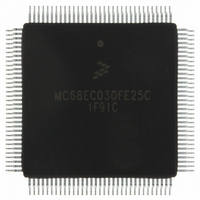
Manufacturer Part Number
MC68EC030FE25C
Description
IC MPU 32 BIT ENHANCED 132-CQFP
Manufacturer
Freescale Semiconductor
Specifications of MC68EC030FE25C
Processor Type
M680x0 32-Bit
Speed
25MHz
Voltage
5V
Mounting Type
Surface Mount
Package / Case
132-CQFP
Family Name
M68000
Device Core
ColdFire
Device Core Size
32b
Frequency (max)
25MHz
Instruction Set Architecture
RISC
Supply Voltage 1 (typ)
5V
Operating Supply Voltage (max)
5.25V
Operating Supply Voltage (min)
4.75V
Operating Temp Range
0C to 70C
Operating Temperature Classification
Commercial
Mounting
Surface Mount
Pin Count
132
Package Type
CQUAD
Lead Free Status / RoHS Status
Contains lead / RoHS non-compliant
Features
-
Lead Free Status / Rohs Status
Compliant
Available stocks
Company
Part Number
Manufacturer
Quantity
Price
Company:

Part Number:
MC68EC030FE25C
Manufacturer:
MOTOROLA
Quantity:
1
Company:
Part Number:
MC68EC030FE25C
Manufacturer:
MOTOROLA
Quantity:
325
Company:
Part Number:
MC68EC030FE25C
Manufacturer:
Freescale Semiconductor
Quantity:
10 000
Part Number:
MC68EC030FE25C
Manufacturer:
MOTOROLA/摩托罗拉
Quantity:
20 000
Company:
Part Number:
MC68EC030FE25CB1
Manufacturer:
Freescale Semiconductor
Quantity:
10 000


2 2
OUTPUTS(1) CLK
OUTPUTS(2) CLK
ALL SIGNALS(5)
INPUTS(3) CLK
INPUTS(4) CLK
NOTES:
LEGEND:
1. This output timing is applicable to all parameters specified relative to the rising edge of the clock.
2. This output timing is applicable to all parameters specified relative to the falling edge of the clock.
3. This input timing is applicable to all parameters specified relative to the rising edge of the clock.
4. This input timing is applicable to all parameters specified relative to the falling edge of the clock.
5. This timing is applicable to all parameters specified relative to the assertion/negation of another signal.
A. Maximum output delay specification.
B. Minimum output hold time.
C. Minimum input setup time specification.
D. Minimum input hold time specification.
E. Signal valid to signal valid specification (maximum or minimum).
F. Signal valid to signal invalid specification (maximum or minimum).
CLK
DRIVE TO
Figure 9.
0.5 V
OUTPUT n
VALID
DRIVE TO
DRIVE TO
0.5 V
2.4 V
Freescale Semiconductor, Inc.
2.0 V
0.8 V
Drive Levels and Test Points for AC Specifications
For More Information On This Product,
B
MC68EC030 TECHNICAL DATA
TO 2.4 V
DRIVE
2.0 V
A
Go to: www.freescale.com
2.0 V
0.8 V
2.0 V
0.8 V
2.0 V
0.8 V
0.8 V
E
F
C
OUTPUT
VALID
INPUT
VALID
2.0 V
0.8 V
OUTPUT n
n + 1
2.0 V
0.8 V
D
VALID
2.0 V
0.8 V
C
INPUT
VALID
2.0 V
0.8 V
2.0 V
B
0.8 V
D
2.0 V
0.8 V
A
2.0 V
0.8 V
M O T O R O L A
VALID
OUTPUT n+1
DRIVE
TO 2.4 V
DRIVE
TO 0.5 V
Related parts for MC68EC030FE25C
Image
Part Number
Description
Manufacturer
Datasheet
Request
R

Part Number:
Description:
Second-generation 32-bit Enhanced Embedded Controller
Manufacturer:
Freescale Semiconductor, Inc
Datasheet:
Part Number:
Description:
Manufacturer:
Freescale Semiconductor, Inc
Datasheet:
Part Number:
Description:
Manufacturer:
Freescale Semiconductor, Inc
Datasheet:
Part Number:
Description:
Manufacturer:
Freescale Semiconductor, Inc
Datasheet:
Part Number:
Description:
Manufacturer:
Freescale Semiconductor, Inc
Datasheet:
Part Number:
Description:
Manufacturer:
Freescale Semiconductor, Inc
Datasheet:
Part Number:
Description:
Manufacturer:
Freescale Semiconductor, Inc
Datasheet:
Part Number:
Description:
Manufacturer:
Freescale Semiconductor, Inc
Datasheet:
Part Number:
Description:
Manufacturer:
Freescale Semiconductor, Inc
Datasheet:
Part Number:
Description:
Manufacturer:
Freescale Semiconductor, Inc
Datasheet:
Part Number:
Description:
Manufacturer:
Freescale Semiconductor, Inc
Datasheet:
Part Number:
Description:
Manufacturer:
Freescale Semiconductor, Inc
Datasheet:
Part Number:
Description:
Manufacturer:
Freescale Semiconductor, Inc
Datasheet:
Part Number:
Description:
Manufacturer:
Freescale Semiconductor, Inc
Datasheet:
Part Number:
Description:
Manufacturer:
Freescale Semiconductor, Inc
Datasheet: