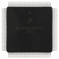
MC68EC030FE25C Freescale Semiconductor, MC68EC030FE25C Datasheet - Page 5

MC68EC030FE25C
Manufacturer Part Number
MC68EC030FE25C
Description
IC MPU 32 BIT ENHANCED 132-CQFP
Manufacturer
Freescale Semiconductor
Specifications of MC68EC030FE25C
Processor Type
M680x0 32-Bit
Speed
25MHz
Voltage
5V
Mounting Type
Surface Mount
Package / Case
132-CQFP
Family Name
M68000
Device Core
ColdFire
Device Core Size
32b
Frequency (max)
25MHz
Instruction Set Architecture
RISC
Supply Voltage 1 (typ)
5V
Operating Supply Voltage (max)
5.25V
Operating Supply Voltage (min)
4.75V
Operating Temp Range
0C to 70C
Operating Temperature Classification
Commercial
Mounting
Surface Mount
Pin Count
132
Package Type
CQUAD
Lead Free Status / RoHS Status
Contains lead / RoHS non-compliant
Features
-
Lead Free Status / Rohs Status
Compliant
Available stocks
Company
Part Number
Manufacturer
Quantity
Price
Company:
Part Number:
MC68EC030FE25C
Manufacturer:
MOTOROLA
Quantity:
1
Company:
Part Number:
MC68EC030FE25C
Manufacturer:
MOTOROLA
Quantity:
325
Company:
Part Number:
MC68EC030FE25C
Manufacturer:
Freescale Semiconductor
Quantity:
10 000
Part Number:
MC68EC030FE25C
Manufacturer:
MOTOROLA/摩托罗拉
Quantity:
20 000
Company:
Part Number:
MC68EC030FE25CB1
Manufacturer:
Freescale Semiconductor
Quantity:
10 000
M O T O R O L A
The ACU contains two access control registers that are used to define memory segments ranging in size
from 16 Mbytes to 2 Gbytes each. Each segment is definable in terms of address, read/write access, and
function code. Each segment can be marked as cacheable or non cacheable to control cache accesses
to that memory space.
As shown in the programming models (see Figures 3 and 4), the MC68EC030 has 16 32-bit general-
purpose registers, a 32-bit program counter, two 32-bit supervisor stack pointers, a 16-bit status register,
a 32-bit vector base register, two 3-bit alternate function code registers, two 32-bit cache handling
(address and control) registers, and two 32-bit transparent translation registers. Registers D0–D7 are
used as data registers for bit and bit field (1 to 32 bit), byte (8 bit), word (16 bit), long-word (32 bit), and
quad-word (64 bit) operations. Registers A0–A6 and the user, interrupt, and master stack pointers are
address registers that may be used as software stack pointers or base address registers. In addition, the
address registers may be used for word and long-word operations. All 16 general-purpose registers (D0–
D7, A0–A7) can be used as index registers.
31
31
31
31
Freescale Semiconductor, Inc.
PROGRAMMING MODEL
For More Information On This Product,
Figure 3. User Programming Model
MC68EC030 TECHNICAL DATA
Go to: www.freescale.com
16
16
16
15
15
15
15
0
8
8
7
7
0
0
0
0
0
D0
D1
D2
D3
D4
D5
D6
D7
(USP)
PC
CCR
A0
A1
A2
A3
A4
A5
A6
A7
DATA
REGISTERS
ADDRESS
REGISTERS
USER STACK
POINTER
PROGRAM
COUNTER
CONDITION CODE
REGISTER
5


