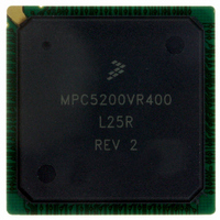
MPC5200VR400 Freescale Semiconductor, MPC5200VR400 Datasheet - Page 21

MPC5200VR400
Manufacturer Part Number
MPC5200VR400
Description
IC MPU 32BIT 400MHZ PPC 272-PBGA
Manufacturer
Freescale Semiconductor
Datasheet
1.MPC5200CVR400B.pdf
(80 pages)
Specifications of MPC5200VR400
Processor Type
MPC52xx PowerPC 32-Bit
Speed
400MHz
Voltage
1.5V
Mounting Type
Surface Mount
Package / Case
272-PBGA
Lead Free Status / RoHS Status
Lead free / RoHS Compliant
Features
-
Available stocks
Company
Part Number
Manufacturer
Quantity
Price
Company:
Part Number:
MPC5200VR400
Manufacturer:
Freescale Semiconductor
Quantity:
135
Company:
Part Number:
MPC5200VR400
Manufacturer:
FRRESCAL
Quantity:
838
Company:
Part Number:
MPC5200VR400
Manufacturer:
MOTOLOLA
Quantity:
648
Company:
Part Number:
MPC5200VR400
Manufacturer:
Freescale Semiconductor
Quantity:
10 000
Company:
Part Number:
MPC5200VR400B
Manufacturer:
TI
Quantity:
233
Company:
Part Number:
MPC5200VR400B
Manufacturer:
Freescale Semiconductor
Quantity:
10 000
Company:
Part Number:
MPC5200VR400BR2
Manufacturer:
Freescale Semiconductor
Quantity:
10 000
3.3.5.3
The SDRAM Memory Controller uses an internally skewed clock for reading DDR memory. The
programmable bits in the Reset Configuration Register used to account for unknown board delays are in
the CDM module. The internal read clock can be delayed up to 3 ns under worst operating conditions in
32 increments of 95 ps, (1.4 ns in 45 ps increments under best case operating conditions) by programming
the CDM Reset Configuration Register tap delay bits. Note: These bits in the CDM Reset Configuration
register are not ‘reset configured’ but have a hard coded reset value and are writable during operation.
Freescale Semiconductor
data
t
data
DM
DM
mem_clk
MBA (Bank Selects)
Sym
t
t
valid
hold
DQM (Data Mask)
valid
hold
valid
hold
Control Signals
MA (Address)
NOTE: Control Signals are composed of RAS, CAS, MEM_WE, MEM_CS, MEM_CS1 and CLK_EN
MDQ (Data)
Memory Interface Timing-DDR SDRAM Read Command
MEM_CLK
MEM_CLK period
Control Signals, Address and MBA Valid
after rising edge of MEM_CLK
Control Signals, Address and MBA Hold after
rising edge of MEM_CLK
DQM valid after rising edge of MEM_CLK
DQM hold after rising edge of Mem_clk
MDQ valid after rising edge of MEM_CLK
MDQ hold after rising edge of MEM_CLK
Figure 6. Timing Diagram—Standard SDRAM Memory Write Timing
t
t
Description
t
valid
valid
valid
Table 19. Standard SDRAM Write Timing
Active
Row
t
t
t
hold
hold
hold
data
DM
valid
valid
MPC5200 Data Sheet, Rev. 4
NOP
WRITE
Column
t
t
mem_clk
mem_clk
t
mem_clk
DM
NOP
Min
data
7.5
—
—
—
*0.25-0.7
*0.75-0.7
hold
*0.5
hold
NOP
t
t
Electrical and Thermal Characteristics
t
mem_clk
mem_clk
mem_clk
NOP
Max
—
—
—
—
*0.25+0.4
*0.75+0.4
*0.5+0.4
NOP
Units
ns
ns
ns
ns
ns
ns
ns
NOP
SpecID
A5.10
A5.11
A5.12
A5.13
A5.14
A5.8
A5.9
21


