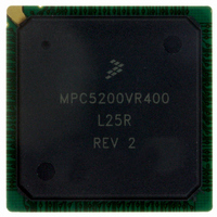
MPC5200VR400 Freescale Semiconductor, MPC5200VR400 Datasheet - Page 52

MPC5200VR400
Manufacturer Part Number
MPC5200VR400
Description
IC MPU 32BIT 400MHZ PPC 272-PBGA
Manufacturer
Freescale Semiconductor
Datasheet
1.MPC5200CVR400B.pdf
(80 pages)
Specifications of MPC5200VR400
Processor Type
MPC52xx PowerPC 32-Bit
Speed
400MHz
Voltage
1.5V
Mounting Type
Surface Mount
Package / Case
272-PBGA
Lead Free Status / RoHS Status
Lead free / RoHS Compliant
Features
-
Available stocks
Company
Part Number
Manufacturer
Quantity
Price
Company:
Part Number:
MPC5200VR400
Manufacturer:
Freescale Semiconductor
Quantity:
135
Company:
Part Number:
MPC5200VR400
Manufacturer:
FRRESCAL
Quantity:
838
Company:
Part Number:
MPC5200VR400
Manufacturer:
MOTOLOLA
Quantity:
648
Company:
Part Number:
MPC5200VR400
Manufacturer:
Freescale Semiconductor
Quantity:
10 000
Company:
Part Number:
MPC5200VR400B
Manufacturer:
TI
Quantity:
233
Company:
Part Number:
MPC5200VR400B
Manufacturer:
Freescale Semiconductor
Quantity:
10 000
Company:
Part Number:
MPC5200VR400BR2
Manufacturer:
Freescale Semiconductor
Quantity:
10 000
Electrical and Thermal Characteristics
3.3.14 J1850
See the MPC5200 User Manual [1].
52
NOTES:
1
2
3
Programming IFDR with the maximum frequency (IFDR=0x20) results in the minimum output timings listed. The
I
position is affected by the prescale and division values programmed in IFDR.
Because SCL and SDA are open-drain-type outputs, which the processor can only actively drive low, the time SCL
or SDA takes to reach a high level depends on external signal capacitance and pull-up resistor values
Inter Peripheral Clock is defined in the MPC5200 User Manual [1].
Sym
2
SCL
SDA
1
2
3
4
5
6
7
8
9
C interface is designed to scale the data transition time, moving it to the middle of the SCL low period. The actual
1
1
2
1
1
1
1
1
1
Start condition hold time
Clock low period
SCL/SDA rise time
Data hold time
SCL/SDA fall time
Clock high time
Data setup time
Start condition setup time (for repeated start condition
only)
Stop condition setup time
1
Table 41. I
Output timing was specified at a nominal 50 pF load.
2
Figure 37. Timing Diagram—I
Description
2
C Output Timing Specifications—SCL and SDA
4
MPC5200 Data Sheet, Rev. 4
6
NOTE
7
2
C Input/Output
Min
10
10
20
10
—
—
6
7
2
8
5
Max
7.9
7.9
—
—
—
—
—
—
—
3
IP-Bus Cycle
IP-Bus Cycle
IP-Bus Cycle
IP-Bus Cycle
IP-Bus Cycle
IP-Bus Cycle
IP-Bus Cycle
Units
Freescale Semiconductor
ns
ns
9
3
3
3
3
3
3
3
SpecID
A13.10
A13.11
A13.12
A13.13
A13.14
A13.15
A13.16
A13.8
A13.9


