Z8038018FSG Zilog, Z8038018FSG Datasheet
Z8038018FSG
Specifications of Z8038018FSG
Available stocks


Related parts for Z8038018FSG


Z8038018FSG Summary of contents
Page 1
... Data Communications Family Z380 Microprocessor Product Specification PS010002-0708 ® Copyright ©2008 by Zilog , Inc. All rights reserved. www.zilog.com ...
Page 2
... Z8, Z8 Encore!, Z8 Encore! XP, Z8 Encore! MC, Crimzon, eZ80, and ZNEO are trademarks or registered trademarks of Zilog, Inc. All other product or service names are the property of their respective owners. PS010002-0708 Z380 Microprocessor ...
Page 3
Revision History Each instance in Revision History reflects a change to this document from its previous revision. For more details, refer to the corresponding pages and appropriate links in the table below. Date Revision Level July 2008 02 March 2001 ...
Page 4
FEATURES • Static CMOS Design with Low-Power Standby Mode Option • 32-Bit Internal Data Paths and ALU • Operating Frequency DC-to-18 MHz at 5V – – DC-to-10 MHz at 3.3V • Enhanced Instruction Set that Maintains Object-Code Compatibility with Z80 ...
Page 5
GENERAL DESCRIPTION The Z380 Microprocessor is an integrated high-performance microprocessor with fast and efficient throughput and increased memory addressing capabilities. The Z380 offers a con- tinuing growth path for present Z80-or Z180-based designs, while maintaining Z80 and Z180 MPU object-code ...
Page 6
All signals with a preceding front slash, "/", are active Low e.g., B//W (WORD is active Note: Low); B/W is active Low, only) Power connections follow conventional descriptions below: Connection Power Ground Clock with Standby Control Chip Selects and Waits ...
Page 7
VSS VDD VSS 10 VDD /TREFR /TREFA /TREFC /BHEN /BLEN 15 /MRD /MWR /MSIZE /WAIT BUSCLK 20 IOCLK /M1 /IORQ /IORD CLKI 25 CLKO /IOWR VSS VDD 30 VSS Figure ...
Page 8
PIN DESCRIPTION A31-A0 Address Bus (outputs, activeHigh, tri-state).These non-multiplexed address sig- nals provide a linear memory address space of four gigabytes. The 32-address signals are also used to access I/O devices. /BACK Bus Acknowledge (output, active Low, tri-state). This signal, ...
Page 9
Evaluation Mode (input, active Low). This input should be left unconnected for nor- /EV mal operation. When it is driven to logic 0, the Z380 MPU conditions itself in the reset mode and tri-states all of its output pin drivers. ...
Page 10
BHEN and /BLEN control signals. /MRD is active from the end of T1 until the end of T4 during memory read transactions. Memory Size (input, active Low). This input, from the addressed memory loca- /MSIZE tion, indicates ...
Page 11
Table 1. Z380 MPU Pin Conditioning Characteristics Operation Mode Conditions Pin Names CLKI CLKO CLKSEL BUSCLK IOCLK A31-A0 D15-D0 /TREFR,/TREFA, /TREFC /MRD,/MWR /BHEN,/BLEN /LMCS,/UMCS, /MCS3-MCS0 /MSIZE,/WAIT /HALT,/STNBY /M1,/INTAK /IORQ,/IORD, /IOWR /BREQ /BACK /NMI,/INT3-/INT0 /RESET / EXTERNAL ...
Page 12
Transactions A transaction is initiated by the bus master and is responded to by some other device on the bus. Only one transaction can proceed at a time; six kinds of transactions can occur: Memory, Refresh, I/O, Interrupt Acknowledge, RETI ...
Page 13
T1 BUSCLK ADDRESS DATA STATUS /WAIT /MSIZE /TREFR /TREFA /TREFC /MRD /MWR PS010002-0708 T2 T3 Figure 3. Read Cycle, No Waits Z380 Microprocessor Product Specification T4 Page 13 of 125 ...
Page 14
T1 BUSCLK ADDRESS DAT A STATUS /WAIT /MSIZE /TREFR /TREFA /TREFC /MRD /MWR PS010002-0708 T1L T1H T2 Figure 4. Read Cycle, T1 Wait Z380 Microprocessor Product Specification T3 T4 Page 14 of 125 ...
Page 15
T1 BUSCLK ADDRESS DAT A STATUS /WAIT /MSIZE /TREFR /TREFA /TREFC /MRD /MWR PS010002-0708 (Continued) T2 T2H T2L Figure 5. Read Cycle, T2 Wait Z380 Microprocessor Product Specification T3 T4 Page 15 of 125 ...
Page 16
T1 BUSCLK ADDRESS DAT A STATUS /WAIT /MSIZE /TREFR /TREFA /TREFC /MRD /MWR PS010002-0708 T2 T3 T3L Figure 6. Read Cycle, T3 Wait Z380 Microprocessor Product Specification T3H T4 Page 16 of 125 ...
Page 17
EXTERNAL INTERFACE (Continued) Write memory transactions are shown without wait states, with wait states between T1 and T2, between T2 and T3, and between T3 and T4 (Figures 7-10). The /MWR strobe is acti- vated at the end of T1, ...
Page 18
T1 BUSCLK ADDRESS DAT A STATUS /WAIT /MSIZE /TREFR /TREFA /TREFC /MRD /MWR PS010002-0708 T1L T1H T2 Figure 8. Write Cycle, T1 Wait Z380 Microprocessor Product Specification T3 T4 Page 18 of 125 ...
Page 19
T1 BUSCLK ADDRESS DAT A STATUS /WAIT /MSIZE /TREFR /TREFA /TREFC /MRD /MWR PS010002-0708 T2 T2H T2L Figure 9. Write Cycle, T2 Wait Z380 Microprocessor Product Specification T3 T4 Page 19 of 125 ...
Page 20
T1 BUSCLK ADDRESS DAT A STATUS /WAIT /MSIZE /TREFR /TREFA /TREFC /MRD /MWR PS010002-0708 T2 T3 T3L Figure 10. Write Cycle, T3 Wait Z380 Microprocessor Product Specification T3H T4 Page 20 of 125 ...
Page 21
EXTERNAL INTERFACE (Continued) Refresh Transactions A memory refresh transaction is generated by the Z380 MPU refresh controller and can occur immediately after the final clock cycle of any other transaction. The address during the refresh transaction is not defined as ...
Page 22
T1 BUSCLK ADDRESS DATA STATUS /WAIT /MSIZE /TREFR /TREFA /TREFC /MRD /MWR PS010002-0708 T2 T3 Figure 12. Refresh Cycle, No Waits Z380 Microprocessor Product Specification T4 Page 22 of 125 ...
Page 23
T1 BUSCLK ADDRESS DAT A STATUS /WAIT /MSIZE /TREFR /TREFA /TREFC /MRD /MWR PS010002-0708 T1L T1H T2 Figure 13. Refresh Cycle, T1 Wait Z380 Microprocessor Product Specification T3 T4 Page 23 of 125 ...
Page 24
T1 BUSCLK ADDRESS DAT A STATUS /WAIT /MSIZE /TREFR /TREFA /TREFC /MRD /MWR PS010002-0708 T2 T2H T2L Figure 14. Refresh Cycle, T2 Wait Z380 Microprocessor Product Specification T3 T4 Page 24 of 125 ...
Page 25
T1 BUSCLK ADDRESS DAT A STATUS /WAIT /MSIZE /TREFR /TREFA /TREFC /MRD /MWR PS010002-0708 T2 T3 T3L Figure 15. Refresh Cycle, T3 Wait Z380 Microprocessor Product Specification T3H T4 Page 25 of 125 ...
Page 26
I/O Transactions I/O transactions move data to or from an external peripheral when the Z380 MPU per- forms an I/O access. All I/O transactions occur referenced to the IOCLK signal, when divided-down version of the BUSCLKsignal. BUSCLK ...
Page 27
I/O Read transactions are shown with and without a wait state (Figures 17-18). The con- tents of the data bus is latched immediately before the falling edge of IOCLK during the last IOCLK cycle of the transaction. IOCLK ADDRESS DAT ...
Page 28
IOCLK ADDRESS DAT A /WAIT /MI /IORQ /IORD /IOWR /INTAK PS010002-0708 Figure 18. I/O Read Cycle, T1 Wait Z380 Microprocessor Product Specification Page 28 of 125 ...
Page 29
EXTERNAL INTERFACE (Continued) I/O Write transactions are shown with and without a wait state (Figures 19-20). The data bus is driven throughout the transaction. IOCLK ADDRESS DAT A /WAIT /MI /IORQ /IORD /IOWR /INTAK PS010002-0708 Figure 19. I/O Write Cycle, ...
Page 30
Z ILOG IOCLK ADDRESS DAT A /WAIT /MI /IORQ /IORD /IOWR /INTAK PS010002-0708 Figure 20. I/O Write Cycle, T1 Wait Z380 Microprocessor Product Specification M ICROPROCE Page 30 of 125 ...
Page 31
EXTERNAL INTERFACE (Continued) Interrupt Acknowledge Transactions An interrupt acknowledge transaction is generated by the Z380 MPU in response to an unmasked external interrupt request. Figure 21 shows an interrupt acknowledge transac- tion in response to /INT0 and Figure 22 shows ...
Page 32
IOCLK ADDRESS DAT A /WAIT /MI /IORQ /IORD /IOWR /INTAK Figure 22. Interrupt Acknowledge Cycle, /INT3-1 An interrupt acknowledge transaction for /INT0 is five IOCLK cycles long unless extended by Wait states. /WAIT is sampled at two separate points during ...
Page 33
An interrupt acknowledge transaction in response to one of /INT3-/INT1 is also five IOCLK cycles long, unless extended by wait states. The waits are sampled and inserted at similar locations as an interrupt acknowledge transaction is for /INT0. Note, however, ...
Page 34
IOCLK ADDRESS DATA /WAIT /M1 /IORQ /IORD /IOWR /INTAK Figure 23. Return From Interrupt Cycle The RETI transaction is ten IOCLK cycles long unless extended by Wait states, and /WAIT is sampled at three separate points during the ...
Page 35
HALT Transactions A HALT transaction occurs whenever the Z380 MPU executes a Halt instruction, with the /HALT signal activated on the falling edge of BUSCLK. If the standby mode is not enabled, executing a Sleep instruction would also cause a ...
Page 36
THH BUSCLK ADDRESS DATA STATUS /WAIT /MSIZE /TREFR /TREFA /TREFC /MRD /MWR /HALT /INT or /NMI PS010002-0708 THL THH THL Figure 25. HALT Exit Z380 Microprocessor Product Specification THH T6 Page 36 of 125 ...
Page 37
Requests A request can be initiated by a device that does not have control of the bus. Two types of request can occur: Bus request and Interrupt request. When an interrupt or bus request is made answered by ...
Page 38
BUSCLK ADDRESS DAT A STATUS /WAIT /MSIZE /TREFR /TREFA /TREFC /MRD /MWR /BREQ /BACK /MI /IORQ /IORD /IOWR /INTAK Figure 26. Bus Request/Acknowledge Cycle PS010002-0708 Transaction in progress T7 Z380 Microprocessor Product Specification TBL Page 38 of 125 ...
Page 39
TBH BUSCLK ADDRESS DATA STATUS /WAIT /MSIZE /TREFR /TREFA /TREFC /MRD /MWR /BREQ /BACK /MI /IORQ /IORD /IOWR /INTAK Figure 27. Bus Request/Acknowledge End Cycle PS010002-0708 TBL TBH TBL Z380 Microprocessor Product Specification TBH TIL Page 39 of 125 ...
Page 40
EXTERNAL INTERFACE (Continued) Miscellaneous Timing There are two cases where a specific transaction is not taking place on the bus which are illustrated in this section: the bus idle cycle and the I/O heartbeat cycle. Idle Cycles When no transactions ...
Page 41
I/O Heartbeat Cycle The Z380 MPU is capable of generating an I/O heartbeat cycle on the I/O bus in response to an I/O write to an on-chip control register. This cycle is most useful with Z80 family peripherals, where some ...
Page 42
EXTERNAL INTERFACE (Continued) Reset Timing The timing for entering and exiting the reset state is shown in Figures 30 and 31. The effects of reset on the internal state of the Z380 MPU are detailed in the Reset section. The ...
Page 43
TRH BUSCLK ADDRESS DAT A STATUS /WAIT /MSIZE /TREFR /TREFA /TREFC /MRD /MWR /IOCTL3-0 /RESET PS010002-0708 TRH TRL TRL Figure 31. Reset Exit Z380 Microprocessor Product Specification TRH TiL Page 43 of 125 ...
Page 44
EXTERNAL INTERFACE (Continued BUSCLK /RESET IOCLK PS010002-0708 Figure 32. IOCLK Reset Start-up Z380 Microprocessor Product Specification Page 44 of 125 ...
Page 45
CPU ARCHITECTURE The Central Processing Unit (CPU) of the Z380 MPU is a binary-compatible extension of the Z80 CPU and Z180 CPU architectures. High throughput rates for the Z380 CPU are achieved by a high clock rate, high bus bandwidth ...
Page 46
Lastly, all word Input/Output operations are performed on 16-bit values. Address Spaces The Z380 CPU architecture supports five distinct address spaces corresponding to the dif- ...
Page 47
Each register set includes the primary registers IX, and IY, as well as the alternate registers A’, F’, B’, C’, D’, E’, H’, L’, IX’, and IY’. These byte registers can be ...
Page 48
IXP (IXPrime Register Select). rently active register selected when this bit is cleared and IX' is selected when this bit is set. Reset clears this bit and selects IX. MAINBANK (Main Bank Select BC, DE, HL, ...
Page 49
The size of the data element being addressed depends on the instruction being executed as well as the Word/Long Word mode. A bit can be addressed by specifying a byte, and a bit within that byte. Bits are numbered from ...
Page 50
CPU ARCHITECTURE (Continued) External I/O Address Space External I/O addresses are generated by I/O instructions, except those reserved for on-chip I/O address space accesses, and can take a variety of forms (Table 2). An I/O read or write is always ...
Page 51
DATA TYPES The Z380 CPU can operate on bits, Binary-Coded Decimal (BCD) digits (4 bits), bytes (8 bits), words (16 bits or 32 bits), byte strings, and word strings. Bits in registers can be set, cleared, and tested. BCD digits, ...
Page 52
This flag is set when an add instruction generates a carry or a subtract instruc- Carry (C). tion generates a borrow. Certain logical, rotate and shift instructions affect the Carry flag. Add/Subtract (N). distinguish between add and subtract operations. The ...
Page 53
Stack Pointer The Stack Pointer (SP) is used for saving information when an interrupt or trap occurs and for supporting subroutine calls and returns. Stack Pointer relative addressing allows parameter passing using the SP. Select Register The Select Register (SR) ...
Page 54
Stack Pointer Relative. adding the two's-complement signed displacement contained in the instruction to the con- tents of the Stack Pointer. Eight bits of index is the norm, but the DDIR IB and DDIR IW decoder directives allow 16-and 24-bit indexes, ...
Page 55
INSTRUCTION SET The Z380 CPU’s instruction set is a superset of the Z80 CPU’s; the Z380 CPU is opcode compatible with the Z80 CPU. Thus a Z80 program can be executed on a Z380 MPU with- out modification. The instruction ...
Page 56
Instruction Set Notation Symbols. The following symbols are used to describe the instruction set. An 8-bit constant 16-bit constant d An 8-bit offset. (2’s complement) r Any one of the CPU register ...
Page 57
Flags. The F register contains the following flags followed by symbols. Sign flag S Z Zero flag H Half carry flag P/V Parity/Overflow flag N Add/Subtract flag C Carry Flag The flag is affected according to the result of the ...
Page 58
Field Encoding The convention for opcode binary format is shown in the following Tables. For example, to get the opcode format on the instruction LD (IX+12h), C; first find out the entry for LD (XY+d),r. That entry has an opcode ...
Page 59
LOAD GROUP Symbolic Mnemonic Operation r ← r’ LD r,r’ r ← r,n LD XYU,n XYU ← XYL,n XYL ← ← (HL) LD r,(HL) r ← (XY+d) LD r,(XY+d) (HL) ← ...
Page 60
LOAD GROUP (Continued) Symbolic Mnemonic Operation LD XYU,s XYU ← XYL,s XYL ← s,XYU s ← XYU LD s,XYL s ← XYL A ← A,I A ← A,R I ← A ...
Page 61
BIT LOAD GROUP Symbolic Mnemonic Operation LD dd, XY, HL,(nn) H (nn+1) L (nn) LD dd,(nn) ddh (nn+1) ddl (nn) LD XY,(nn) XYU (nn+1) XYL (nn) LD (nn),HL (nn+1) H (nn ...
Page 62
BIT LOAD GROUP (Continued) Symbolic Mnemonic Operation LD IY, pp, (pp),XY (pp+1) XYU (pp) XYL LD XY,(pp) XYU (pp+1) XYL (pp) LD pp,(XY+d) pph (XY+d)h ppl (XY+d)l LD IX,(IY+d) IXU (IY+d)h IXL (IY+d)l ...
Page 63
Symbolic Mnemonic Operation LD (SP+d),pp (SP+d)h pph (SP+d)l ppl LD (SP+d),XY (SP+d)h XYU (SP+d)l XYL LD [W] I, [W] HL Pair ...
Page 64
PUSH/POP INSTRUCTIONS Symbolic Mnemonic Operation PUSH qq (SP-2) qql (SP-1) qqh SP SP-2 PUSH XY (SP-2) XYL (SP-1) XYU SP SP-2 PUSH nn (SP-2) nnl (SP-1) nnh SP SP-2 PUSH SR (SP-2) SR(7-0) (SP-1) SR(15-8) SP SP-2 POP qq qqh ...
Page 65
EXCHANGE, BLOCK TRANSFER, BLOCK SEARCH GROUPS Symbolic Mnemonic Operation EX AF, AF’ SR(0) NOT SR(0) EX DE,HL DE(15-0) HL(15-0) EX BC,DE BC(15-0) DE(15-0) EX BC,HL BC(15-0) HL(15-0) EXX SR(8) NOT SR(8) EX (SP),HL H (SP+1) L (SP) EX (SP),XY XYU ...
Page 66
EXCHANGE, BLOCK TRANSFER, BLOCK SEARCH GROUPS (Continued) Symbolic Mnemonic Operation LDDR (DE) (HL) DE DE-1 HL HL-1 BC(15-0) BC(15-0)-1 Repeat until CPI A-(HL) HL HL+1 BC(15-0) BC(15-0)-1 CPIR A-(HL) HL HL+1 BC(15-0) BC(15-0)-1 Repeat until A = ...
Page 67
Symbolic Mnemonic Operation LDDW (DE) (HL) (DE+1) (HL+1) DE DE-2 HL HL-2 BC(15-0) BC(15-0)-2 LDDRW (DE) (HL) (DE+1) (HL+1) DE DE-2 HL HL-2 BC(15-0) BC(15-0)-2 Repeat until Reg pp Regs 000 001 C ...
Page 68
ARITHMETIC AND LOGICAL GROUP Symbolic Mnemonic Operation ADD A ADD A ADD A,(HL (HL) ADD A,(XY+ ( ADD A,XYU XYU ...
Page 69
Symbolic Mnemonic Operation TST r A AND r TST n A AND n TST (HL) A AND (HL) r Reg y 000 B 0 001 C 1 010 D 011 E 100 H 101 L 111 A Notes: Instructions in ...
Page 70
GENERAL PURPOSE ARITHMETIC AND CPU CONTROL GROUP Symbolic Mnemonic Operation DAA @ CPL[A] A NOT A One’s complement CPLW[HL] HL NOT HL One’s complement NEG[A] A 0-A Two’s complement NEGW[HL] HL 0-HL Two’s complement EXTS [ ...
Page 71
Symbolic Mnemonic Operation LDCTL SR,HL SR(15-8) HL(15-8) SR(0) HL(0) if (LW) SR(31-16) HL(31-16) else SR(31-24) HL(15-8) SR(23-16) HL(15-8) LDCTL A LDCTL v LDCTL v SETC LCK SR(1) 1 Set Lock mode SETC LW SR(6) ...
Page 72
DECODER DIRECTIVE INSTRUCTIONS Mnemonic Operation DDIR W Operate following inst in word mode. DDIR IB,W Operate following inst in word mode. Fetching additional byte data. DDIR IW,W Operate following inst in word mode. Fetching additional word data. DDIR IB Fetching ...
Page 73
BIT ARITHMETIC AND LOGICAL GROUP Symbolic Mnemonic Operation ADD HL,dd HL HL+ dd ADC HL HL SBC HL, ADD XY, ADD XY, ...
Page 74
BIT ARITHMETIC AND LOGICAL GROUP (Continued) Symbolic Mnemonic Operation ADDW [HL,] ADDW [HL,]XY HL HL+XY ADDW [HL,](XY+d) HL HL+(XY+d) ADCW [HL,]uu HL HL+uu+CY SUBW [HL,]uu HL HL-uu SBCW [HL,] ...
Page 75
MULTIPLY/DIVIDE INSTRUCTION GROUP Symbolic Mnemonic Operation MLT dd dd ddH * ddL MULTW [HL,]pp HL(31-0) HL(15-0) * pp(15-0) MULTW [HL,]XY HL(31-0) HL(15-0) * XY(15-0) MULTW [HL,]nn HL(31-0) HL(15- MULTW (XY+d) HL(31-0) HL(15-0) * (XY+d) MULTUW uu HL(31-0) HL(15-0) ...
Page 76
MULTIPLY/DIVIDE INSTRUCTION GROUP (Continued) Symbolic Mnemonic Operation DIVUW [HL,]pp HL(15-0) HL(31-0)/pp HL(31-16) DIVUW [HL,]XY HL(15-0) HL(31-0)/XY HL(31-16) DIVUW [HL,]nn HL(15-0) HL(31-0)/nn HL(31-16) DIVUW [HL,](XY+d) HL(15-0) HL(31-0)/(XY+d) HL(31-16) r Reg pp 000 B 00 001 C 00 010 D 11 011 ...
Page 77
ROTATE AND SHIFT GROUP Symbolic Mnemonic Operation RLCA Rotate Left Circular Accumulator RLA Rotate Left Accumulator RRCA Rotate Right Circular Accumulator RRA Rotate Right Accumulator RLC r Rotate Left Circular register r RLC (HL) Rotate Left Circular RLC (XY+d) ...
Page 78
BIT ROTATE AND SHIFT GROUP Symbolic Mnemonic Operation RLCW pp Rotate Left Circular RLCW XY Rotate Left Circular RLCW (HL) Rotate Left Circular RLCW (XY+d) Rotate Left Circular RLW m Rotate Left RRCW m Rotate Right Circular RRW m ...
Page 79
BIT SET, RESET, AND TEST GROUP Symbolic Mnemonic Operation BIT b BIT b,(HL) Z (HL)b BIT b,(XY+d) Z (XY+d)b SET b SET b,(HL) (HL)b 1 SET b,(XY+d) (XY+d)b 1 RES b form ...
Page 80
JUMP GROUP Symbolic Mnemonic Operation JP nn PC(15- (HL) PC(15-0) HL(15-0) JP (XY) PC(15-0) XY(15-0) JP cc,nn If condition cc is true then PC nn otherwise continue C ...
Page 81
Symbolic Mnemonic Operation JR NC,eee continue eee JR Z,eee continue eee JR NZ,eee continue ...
Page 82
CALL AND RETURN GROUP Symbolic Mnemonic Operation CALL nn (SP-1) PCh (SP-2) PCl SP SP CALL cc,nn If condition cc is false continue otherwise same as CALL nn CALR e (SP-1) PCh (SP-2) PCl SP SP ...
Page 83
Symbolic Mnemonic Operation RETN Return from NMI RST p (SP-1) PCh (SP-2) PCl SP SP-2 PCh 0 PCl p cc Condition 000 NZ (Non-zero) 001 Z (Zero) 010 NC (Non-carry) 011 C (Carry) 100 PO (Parity Odd (Non-Overflow) ...
Page 84
INPUT AND OUTPUT GROUP Symbolic Mnemonic Operation IN A,(n) A (n) IN r,(C) r (C) INA A,(nn) A (nn) INI (HL) ( INIR (HL) ( ...
Page 85
Symbolic Mnemonic Operation OUTI B ¨ B-1 (C) (HL OTIR B B-1 (C) (HL) HL ¨ Repeat until OUTD B B-1 (C) (HL) HL ¨ Repeat until ...
Page 86
INPUT AND OUTPUT INSTRUCTIONS FOR ON-CHIP I/O SPACE Symbolic Mnemonic Operation INO r,(n) r (n) INO (n) r (n) Changes Flag only. OUT0 (n),r (n) r TSTIO n (C) AND n OTIIM (C) (HL C+1 ...
Page 87
INPUT AND OUTPUT GROUP Symbolic Mnemonic Operation INW pp,(C) pp (C) INAW HL,(nn) HL(15-0) (nn) INIW (HL) (DE) BC(15-0) BC(15- HL+2 INIRW (HL) (DE) BC(15-0) BC(15- HL+2 Repeat until INDW ...
Page 88
INPUT AND OUTPUT GROUP (Continued) Symbolic Mnemonic Operation OUTDW BC(15-0) BC(15- (DE) (HL OTDRW BC(15-0) BC(15- (DE) (HL Repeat until ppp Reg 000 BC ...
Page 89
INTERRUPTS The Z380 MPU’s interrupt structure provides compatibility with the existing Z80 and Z180 MPUs with the following exception: The undefined opcode trap’s occurrence is with respect to the Z380 instruction set, and its response is improved (vs the Z180) ...
Page 90
Interrupt Control The Z380 MPU’s flags and registers associated with inter- rupt processing are listed in Table 4. As discussed in the CPU Architecture section, some of the registers reside in Names Interrupt Enable Flags Interrupt Register Interrupt Register Extension ...
Page 91
Interrupt Enable Register IE3-IE0 (Interrupt Request Enable Flags). These flags individually indicate F /INT3, /INT2, /INT1 or /INT0 is enabled. Note that these flags are conditioned with enable and disable interrupt instructions (with arguments). IER: 00000017H Read Only 7 -- ...
Page 92
Trap and Break Register Reserved bits 7-2. Some of these bits are reserved for breakpoint functions, including a Break-on-Halt feature. TRPBK: 00000019H R (Trap on Instruction Fetch). TF goes active to logic 1 when ...
Page 93
Nonmaskable Interrupt The nonmaskable interrupt input /NMI is edge sensitive, with the Z380 MPU internally latching the occurrence of its falling edge. When the latched version of /NMI is recog- nized, the following operations are performed. 1. The interrupted PC ...
Page 94
Assigned Interrupt Vectors Mode For Maskable interrupt INT3-/INT1 When the Z380 MPU recognizes one of the external maskable interrupts it generates an Interrupt Acknowl- edge transaction which is different than that for /INT0. The Interrupt Acknowledge transaction for /INT3-/INT1 has ...
Page 95
ON-CHIP PERIPHERAL FUNCTIONS The Z380 MPU incorporates a number of functions to ease its interface with external I/O devices and with various types of memories. The Z380 MPU's I/O bus can be programmed to run at a slower rate than ...
Page 96
I/O Bus Control Register 1 When this phantom register IOCR1 with address 00000012H is accessed with one of the on-chip I/O write instructions, a heartbeat transaction that emulates a Z80 CPU instruction fetch is performed on the I/O bus. This ...
Page 97
MEMORY CHIP SELECTS AND WAITS The Z380 MPU offers two schemes to generate chip select signals to access the lowest 16 Mbytes of its memory address space. The first scheme provides six chip select signals, with the address space partitioned ...
Page 98
Lower Memory Chip Select Control This memory area has its lower boundary at address 000000000H. A user can define the size integer power of two, starting at 4 Kbytes. For example, the lower memory area can be ...
Page 99
Upper Memory Chip Select Control The upper boundary for this memory area is address 00FFFFFFH. A user can define the area immediately below this boundary with a size that is an integer power of two, starting at 4 Kbytes. That ...
Page 100
Mid-range Memory Chip Select(s) Control In chip select scheme 1, a user can define the base address and the total size of the mid-range memory area. The /MCS0 signal would be active for the lowest quarter portion of the area ...
Page 101
BA23-BA14 (Base Address 23-14). In chip select scheme 1, the address signals A23-A16 of a memory transaction are compared with BA23-BA16 for a match, for those bits programmed for address matching in the Mid-range Memory Chip Select Register 1. The ...
Page 102
Mid-range Memory Wait Register 0 T1W2-T1W0 (T1 Waits). This binary field defines up to seven T1 wait states to be inserted in transactions accessing the mid-range memory area 0 in chip select scheme 1, or the entire mid-range memory area ...
Page 103
Mid-Range Memory Wait Register 2 T1W2-T1W0 (T1 Waits). This binary field defines up to seven T1 wait states to be inserted in transactions accessing the mid-range memory area 2 in chip select scheme 1. T2W1-T2W0 (T2 Waits). This binary field ...
Page 104
Memory Chip Selects and Waits Master Control The memory chip selects and their associated waits are enabled or disabled by writing to a single register de- scribed in the following: MSMER: 00000010H R/W 7 ENUM ENM1 ENM2 ENLM 1 1 ...
Page 105
DRAM Refresh The Z380 MPU is capable of providing refresh transactions to dynamic memories that have internal refresh address counters. A user can select how often refresh requests should be made to the Z80 MPU's External Interface Logic, as well ...
Page 106
Refresh Register 2 RFEN (Refresh Enable). Enables the refresh function when programmed to logic 1. Reserved bit 6. Read as 0, should write BS5-BS0 (Burst Size). This field defines the number of refresh transactions per refresh request ...
Page 107
LOW POWER STANDBY MODE The Z380 MPU provides an optional standby mode to minimize power consumption during system idle time. If this option is enabled, executing the Sleep instruction would stop clocking internal to the Z380 MPU, as well as ...
Page 108
Standby Mode Exit With Bus Request Optionally, if the BRXT bit of the Standby Mode Control Register (SMCR) was previously set, /STNBY goes to logic 1 when the /BREQ input is asserted, allowing the external crystal oscillator that drives the ...
Page 109
Standby Mode Entering Timing Figure 53 shows standby mode entering timing in an example where IOCLK was programmed to be BUSCLK BUSCLK IOCLK /STNBY ADDRESS DATA BUS CNTLS Standby Mode Exit With Reset When /RESET is asserted, /STNBY goes to ...
Page 110
Standby Mode Exit With External Interrupts Standby mode can be exited by asserting input /NMI. Asserting the maskable interrupt inputs /INT3-/INT0 may also exit standby mode, if the global interrupt flag IEF1 was previously enabled at logic 1, and for ...
Page 111
Standby Mode for On-chip Crystal Oscillator The previous discussions have been focused on situations where a direct clock is supplied to the Z380 MPU's CLKI input. Such a clock may be sourced by an external crystal with its oscillation circuit. ...
Page 112
RESET The Z380 MPU is placed in a dormant state when the /RESET input is asserted. All its operations are terminated, including any interrupt, bus request or bus transaction that may be in progress. Its IOCLK goes Low on the ...
Page 113
Table 7. Effect of a Reset on Z380 CPU and Related I/O Registers Register Program Counter Stack Pointer I R Select Register A and F Registers Register Extensions I/O Bus Control Register 0 Interrupt Enable Register Assigned Vector Base Register ...
Page 114
ABSOLUTE MAXIMUM RATINGS Voltage on V with respect to V .......... –0.3V to +7. Voltage on all pins, with respect to V .................... –0. Operating Ambient Temperature: .................. 0 to +70°C Storage Temperature: ........................... –55°C ...
Page 115
AC CHARACTERISTICS ™ Z380 Version No. Symbol Parameter 1 TcC CLK Cycle Time 2 TwCh CLK Width High 3 TwCl CLK Width Low 4 TrC CLK Rise Time 5 TfC CLK Fall Time 6 TdCf(BCr) CLK Fall to BUSCLK Rise ...
Page 116
DC CHARACTERISTICS Low Voltage Z380 ™ Version Symbol Parameter V Input High Voltage IH V Input Low Voltage IL V Output High Voltage (–200 µA I OH1 V Output Low Voltage (1 Input Leakage Current IL ...
Page 117
AC CHARACTERISTICS Low Voltage Z380 ™ No. Symbol Parameter 1 TcC CLK Cycle Time 2 TwCh CLK Width High 3 TwCl CLK Width Low 4 TrC CLK Rise Time 5 TfC CLK Fall Time 6 TdCf(BCr) CLK Fall to BUSCLK ...
Page 118
AC CHARACTERISTICS (Continued) CLK 5 BUSCLK 6 OUTPUT OUTPUT INPUT INPUT /NMI /RESET Figure 56. Z380™ CPU Timing Page ...
Page 119
APPENDIX A no esc ED esc DD esc 00 NOP IN0 B,( BC,nn OUT0 (n), (BC),A LD BC,BC 03 INC BC,IX 04 INC B TST B 05 DEC B EX BC, ...
Page 120
APPENDIX A (Continued) no esc ED esc DD esc 31 LD SP, (nn),A LD HL,BC 33 INC HL,IX 34 INC (HL) TST (HL) 35 DEC (HL (HL),n LD (HL),nn 37 SCF ...
Page 121
ED esc DD esc 66 LD H,(HL H,(IX+ H,A RRD LD IXU L,B IN L,(C) LD IXL L,C OUT (C),L LD IXL L,D ADC HL,HL LD IXL,D 6B ...
Page 122
APPENDIX A (Continued) no esc ED esc DD esc 98 SBC A SBC A SBC A SBC A,E OTDMR - 9C SBC A,H SBCW BC SBC A,IXU 9D SBC A,L SBCW ...
Page 123
ED esc escape escape CC CALL Z,nn CALR Z,e CD CALL nn CALR e CE ADC A RST 1 BTEST D0 RET NC LDCTL A,DSR D1 POP ...
Page 124
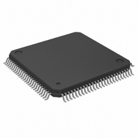
PACKAGE INFORMATION 100-Lead QFP Package Diagram Page 124 of 125 ...
Page 125
... Package Speed Product Number Zilog Prefix © 1997 by Zilog, Inc. All rights reserved. No part of this document may be copied or reproduced in any form or by any means without the prior written consent of Zilog, Inc. The information in this document is subject to change without notice. Devices sold by Zilog, Inc ...