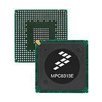
MPC8313VRADDB Freescale Semiconductor, MPC8313VRADDB Datasheet - Page 42

MPC8313VRADDB
Manufacturer Part Number
MPC8313VRADDB
Description
MPU POWERQUICC II PRO 516-PBGA
Manufacturer
Freescale Semiconductor
Datasheet
1.MPC8313CZQAFFB.pdf
(100 pages)
Specifications of MPC8313VRADDB
Processor Type
MPC83xx PowerQUICC II Pro 32-Bit
Speed
267MHz
Voltage
0.95 V ~ 1.05 V
Mounting Type
Surface Mount
Package / Case
516-PBGA
Processor Series
MPC8xxx
Core
e300
Data Bus Width
32 bit
Development Tools By Supplier
MPC8313E-RDB
Maximum Clock Frequency
400 MHz
Operating Supply Voltage
- 0.3 V to + 1.26 V
Maximum Operating Temperature
+ 105 C
Mounting Style
SMD/SMT
Data Ram Size
16 KB
I/o Voltage
2.5 V
Interface Type
I2C, SPI, UART
Minimum Operating Temperature
- 40 C
Program Memory Type
EEPROM/Flash
Lead Free Status / RoHS Status
Lead free / RoHS Compliant
Features
-
Lead Free Status / Rohs Status
Lead free / RoHS Compliant
Available stocks
Company
Part Number
Manufacturer
Quantity
Price
Company:
Part Number:
MPC8313VRADDB
Manufacturer:
MOTOLOLA
Quantity:
885
Company:
Part Number:
MPC8313VRADDB
Manufacturer:
Freescale Semiconductor
Quantity:
10 000
High-Speed Serial Interfaces (HSSI)
Figure 29
Since LVPECL driver’s DC levels (both common mode voltages and output swing) are incompatible with
the MPC8313E SerDes reference clock input’s DC requirement, AC coupling has to be used.
assumes that the LVPECL clock driver’s output impedance is 50 Ω. R1 is used to DC-bias the LVPECL
outputs prior to AC coupling. Its value could be ranged from 140 to 240 Ω depending on the clock driver
vendor’s requirement. R2 is used together with the SerDes reference clock receiver’s 50-Ω termination
resistor to attenuate the LVPECL output’s differential peak level such that it meets the MPC8313E
SerDes3 reference clock’s differential input amplitude requirement (between 200 and 800 mV differential
peak). For example, if the LVPECL output’s differential peak is 900 mV and the desired SerDes reference
clock input amplitude is selected as 600 mV, the attenuation factor is 0.67, which requires R2 = 25 Ω.
Consult with the clock driver chip manufacturer to verify whether this connection scheme is compatible
with a particular clock driver chip.
42
LVPECL CLK Driver Chip
LVDS CLK Driver Chip
Clock Driver
Clock Driver
Clock Driver
Clock Driver
Clock Driver
Figure 29. AC-Coupled Differential Connection with LVPECL Clock Driver (Reference Only)
Figure 28. AC-Coupled Differential Connection with LVDS Clock Driver (Reference Only)
shows the SerDes reference clock connection reference circuits for LVPECL type clock driver.
CLK_Out
CLK_Out
CLK_Out
CLK_Out
CLK_Out
CLK_Out
MPC8313E PowerQUICC
10 nF
10 nF
R1
R1
100 Ω Differential PWB Trace
100 Ω Differential PWB Trace
R2
R2
R2
R2
™
II Pro Processor Hardware Specifications, Rev. 3
10 nF
10 nF
SD n _REF_CLK
SD n _REF_CLK
SD n _REF_CLK
SD n _REF_CLK
50 Ω
50 Ω
50 Ω
50 Ω
Freescale Semiconductor
SerDes Refer.
CLK Receiver
SerDes Refer.
CLK Receiver
MPC8313E
MPC8313E
Figure 29


