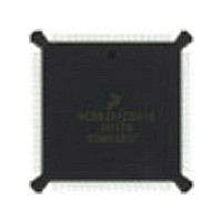
MC68020EH16E Freescale Semiconductor, MC68020EH16E Datasheet - Page 268

MC68020EH16E
Manufacturer Part Number
MC68020EH16E
Description
IC MPU 32BIT 33MHZ 132-PQFP
Manufacturer
Freescale Semiconductor
Datasheet
1.MC68020EH16E.pdf
(306 pages)
Specifications of MC68020EH16E
Processor Type
M680x0 32-Bit
Speed
166MHz
Voltage
5V
Mounting Type
Surface Mount
Package / Case
132-MQFP, 132-PQFP
Family Name
M68000
Device Core
ColdFire
Device Core Size
32b
Frequency (max)
16.67MHz
Instruction Set Architecture
RISC
Supply Voltage 1 (typ)
5V
Operating Supply Voltage (max)
5.25V
Operating Supply Voltage (min)
4.75V
Operating Temp Range
0C to 70C
Operating Temperature Classification
Commercial
Mounting
Surface Mount
Pin Count
132
Package Type
PQFP
Lead Free Status / RoHS Status
Lead free / RoHS Compliant
Features
-
Lead Free Status / Rohs Status
Compliant
Available stocks
Company
Part Number
Manufacturer
Quantity
Price
Company:
Part Number:
MC68020EH16E
Manufacturer:
Freescale Semiconductor
Quantity:
10 000
- Current page: 268 of 306
- Download datasheet (3Mb)
During asynchronous bus cycles, DSACK1 / DSACK0 are used to terminate the current
bus cycle. In true asynchronous operations, such as accesses to peripherals operating at
a different clock frequency, either or both signals may be asserted without regard to the
clock, and then data must be valid a certain amount of time later as defined by
specification 31. With a 25-MHz controller, this time is 32 ns after DSACK1 / DSACK0
asserts; with a 16.67-MHz controller, this time is 50 ns after DSACK1 / DSACK0 asserts
(both numbers vary with the actual clock frequency).
However, many local memory systems do not operate in a truly asynchronous manner
because either the memory control logic can be related to the MC68020/EC020 clock or
worst-case propagation delays are known; thus, asynchronous setup times for the
DSACK1 / DSACK0 signals can be guaranteed. The timing requirements for this pseudo-
synchronous DSACK1 / DSACK0 generation is governed by the equation for t
9-14
Where:
Equation
Equation
t27A
t47A
t27
9-3
9-4
9-5
9-6
9-7
9-8
9-3
9-4
9-5
9-6
9-7
9-8
tX
t1
t2
t3
t6
t9
N = The Total Number of Clock Periods in the Bus Cycle (N
= Refers to AC Electrical Specification X
= The Clock Period
= The Clock Low Time
= The Clock High Time
= The Clock High to Address Valid Time
= The Clock Low to AS Low Delay
= The Data-In to Clock Low Setup Time
= The BERR / HALT to Clock Low Setup Time
= The Asynchronous Input Setup Time
Table 9-4. Memory Access Time Equations at 16.67 and 25 MHz
t
t
t
t
t
t
t
t
t
t
t
t
AVDL
SADL
AVBHL
SABHL
AVDV
SADV
AVDL
SADL
AVBHL
SABHL
AVDV
SADV
= (N – 1) • t1 – t2 – t6 – t47A
= (N – 1) • t1 – t9 – t60
= N • t1 – t2 – t6 – t27
= (N – 1) • t1 – t9 – t27
= (N – 1) • t1 – t2 – t6 – t47A
= (N – 1) • t1 – t9 – t60
= N • t1 – t2 – t6 – t27
= (N – 1) • t1 – t9 – t27
= N • t1 – t2 – t6 – t27A
= (N – 1) • t1 – t9 – t27A
= N • t1 – t2 – t6 – t27A
= (N – 1) • t1 – t9 – t27A
Freescale Semiconductor, Inc.
16.667 MHz
For More Information On This Product,
25 MHz
M68020 USER’S MANUAL
Go to: www.freescale.com
N = 3
N = 3
121
25
85
17
57
61
22
40
31
22
26
71
3 Cycles)
N = 4
N = 4
121
181
145
111
85
46
70
71
57
41
44
97
N = 5
N = 5
181
145
100
241
205
111
151
137
70
97
60
62
N = 6
N = 6
241
205
130
301
265
151
137
191
177
94
79
80
AVDL
N = 7
N = 7
301
265
118
361
325
177
231
217
160
191
98
98
MOTOROLA
.
Unit
Unit
ns
ns
ns
ns
ns
ns
ns
ns
ns
ns
ns
ns
Related parts for MC68020EH16E
Image
Part Number
Description
Manufacturer
Datasheet
Request
R

Part Number:
Description:
(MC600 Series) INTEGRATED CIRCUITS
Manufacturer:
ETC
Datasheet:
Part Number:
Description:
Manufacturer:
Freescale Semiconductor, Inc
Datasheet:
Part Number:
Description:
Manufacturer:
Freescale Semiconductor, Inc
Datasheet:
Part Number:
Description:
Manufacturer:
Freescale Semiconductor, Inc
Datasheet:
Part Number:
Description:
Manufacturer:
Freescale Semiconductor, Inc
Datasheet:
Part Number:
Description:
Manufacturer:
Freescale Semiconductor, Inc
Datasheet:
Part Number:
Description:
Manufacturer:
Freescale Semiconductor, Inc
Datasheet:
Part Number:
Description:
Manufacturer:
Freescale Semiconductor, Inc
Datasheet:
Part Number:
Description:
Manufacturer:
Freescale Semiconductor, Inc
Datasheet:
Part Number:
Description:
Manufacturer:
Freescale Semiconductor, Inc
Datasheet:
Part Number:
Description:
Manufacturer:
Freescale Semiconductor, Inc
Datasheet:
Part Number:
Description:
Manufacturer:
Freescale Semiconductor, Inc
Datasheet:
Part Number:
Description:
Manufacturer:
Freescale Semiconductor, Inc
Datasheet:
Part Number:
Description:
Manufacturer:
Freescale Semiconductor, Inc
Datasheet:
Part Number:
Description:
Manufacturer:
Freescale Semiconductor, Inc
Datasheet:


