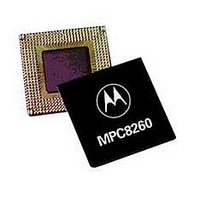
XPC8260CZUHFBC Freescale Semiconductor, XPC8260CZUHFBC Datasheet - Page 21

XPC8260CZUHFBC
Manufacturer Part Number
XPC8260CZUHFBC
Description
IC MPU POWERQUICC II 480-TBGA
Manufacturer
Freescale Semiconductor
Series
PowerQUICC IIr
Specifications of XPC8260CZUHFBC
Processor Type
MPC82xx PowerQUICC II 32-bit
Speed
166MHz
Voltage
2.5V
Mounting Type
Surface Mount
Package / Case
480-TBGA
Core Size
32 Bit
Program Memory Size
32KB
Cpu Speed
133MHz
Embedded Interface Type
I2C, MII, SPI, TDM, UTOPIA
Digital Ic Case Style
TBGA
No. Of Pins
480
Rohs Compliant
No
Family Name
MPC82XX
Device Core
PowerQUICC II
Device Core Size
32b
Frequency (max)
166MHz
Instruction Set Architecture
RISC
Supply Voltage 1 (typ)
1.8V
Operating Supply Voltage (max)
1.9V
Operating Supply Voltage (min)
1.7V
Operating Temp Range
-40C to 105C
Operating Temperature Classification
Industrial
Mounting
Surface Mount
Pin Count
480
Package Type
TBGA
Lead Free Status / RoHS Status
Contains lead / RoHS non-compliant
Features
-
Lead Free Status / Rohs Status
Not Compliant
Available stocks
Company
Part Number
Manufacturer
Quantity
Price
Company:
Part Number:
XPC8260CZUHFBC
Manufacturer:
Freescale Semiconductor
Quantity:
10 000
Figure 11
Freescale Semiconductor
MPC8260A PowerQUICC™ II Integrated Communications Processor Hardware Specifications, Rev. 2.0
shows signal behavior in MEMC mode.
Generally, all MPC826xA bus and system output signals are driven from the
rising edge of the input clock (CLKin). Memory controller signals,
however, trigger on four points within a CLKin cycle. Each cycle is divided
by four internal ticks: T1, T2, T3, and T4. T1 always occurs at the rising
edge, and T3 at the falling edge, of CLKin. However, the spacing of T2 and
T4 depends on the PLL clock ratio selected, as shown in
Figure 12
Memory controller signals
1:2, 1:3, 1:4, 1:5, 1:6
CLKin
CLKin
CLKin
PLL Clock Ratio
Figure 12. Internal Tick Spacing for Memory Controller Signals
1:2.5
1:3.5
T1
T1
T1
is a graphical representation of
Table 11. Tick Spacing for Memory Controller Signals
CLKin
V_CLK
T2
T2
T2
Figure 11. MEMC Mode Diagram
1/4 CLKin
3/10 CLKin
4/14 CLKin
Tick Spacing (T1 Occurs at the Rising Edge of CLKin)
T3
T3
T3
T2
NOTE
T4
T4
T4
1/2 CLKin
1/2 CLKin
1/2 CLKin
Table
sp34/sp30
T3
11.
for 1:2, 1:3, 1:4, 1:5, 1:6
for 1:2.5
for 1:3.5
Table
3/4 CLKin
8/10 CLKin
11/14 CLKin
Electrical and Thermal Characteristics
11.
T4
21


