MPC8313CVRAFFB Freescale Semiconductor, MPC8313CVRAFFB Datasheet - Page 56
MPC8313CVRAFFB
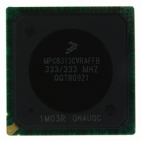
Manufacturer Part Number
MPC8313CVRAFFB
Description
IC MPU POWERQUICC II PRO 516PBGA
Manufacturer
Freescale Semiconductor
Datasheet
1.MPC8313CZQAFFB.pdf
(100 pages)
Specifications of MPC8313CVRAFFB
Processor Type
MPC83xx PowerQUICC II Pro 32-Bit
Speed
333MHz
Voltage
0.95 V ~ 1.05 V
Mounting Type
Surface Mount
Package / Case
516-PBGA
Processor Series
MPC8xxx
Core
e300
Data Bus Width
32 bit
Development Tools By Supplier
MPC8313E-RDB
Maximum Clock Frequency
333 MHz
Operating Supply Voltage
- 0.3 V to + 1.26 V
Maximum Operating Temperature
+ 105 C
Mounting Style
SMD/SMT
I/o Voltage
2.5 V
Interface Type
I2C, SPI, UART
Minimum Operating Temperature
- 40 C
Program Memory Type
EEPROM/Flash
For Use With
MPC8313E-RDB - BOARD PROCESSOR
Lead Free Status / RoHS Status
Lead free / RoHS Compliant
Features
-
Lead Free Status / Rohs Status
Lead free / RoHS Compliant
Available stocks
Company
Part Number
Manufacturer
Quantity
Price
Company:

Part Number:
MPC8313CVRAFFB
Manufacturer:
FREESCAL
Quantity:
120
Company:
Part Number:
MPC8313CVRAFFB
Manufacturer:
Freescale Semiconductor
Quantity:
10 000
Part Number:
MPC8313CVRAFFB
Manufacturer:
FREESCALE
Quantity:
20 000


PCI
14 PCI
This section describes the DC and AC electrical specifications for the PCI bus.
14.1
Table 51
14.2
This section describes the general AC timing parameters of the PCI bus. Note that the PCI_CLK or
PCI_SYNC_IN signal is used as the PCI input clock depending on whether the MPC8313E is configured
as a host or agent device.
Table 52
56
High-level input voltage
Low-level input voltage
High-level output voltage
Low-level output voltage
Input current
Note:
1. Note that the symbol V
Clock to output valid
Output hold from clock
Clock to output high impedance
Input setup to clock
Input hold from clock
Notes:
1. The symbols used for timing specifications follow the pattern of t
2. See the timing measurement conditions in the PCI 2.3 Local Bus Specifications .
3. For purposes of active/float timing measurements, the Hi-Z or off state is defined to be when the total current delivered
4. Input timings are measured at the pin.
.
inputs and t
(PC) with respect to the time the input signals (I) reach the valid state (V) relative to the PCI_SYNC_IN clock, t
(K) going to the high (H) state or setup time. Also, t
(R) went high (H) relative to the frame signal (F) going to the valid (V) state.
through the component pin is less than or equal to the leakage current specification.
provides the DC electrical characteristics for the PCI interface.
shows the PCI AC timing specifications at 66 MHz.
PCI DC Electrical Characteristics
PCI AC Electrical Specifications
Parameter
(first two letters of functional block)(reference)(state)(signal)(state)
Parameter
MPC8313E PowerQUICC
IN
, in this case, represents the OV
Table 52. PCI AC Timing Specifications at 66 MHz
Table 51. PCI DC Electrical Characteristics
Symbol
V
V
V
V
I
OH
IN
OL
IH
IL
™
II Pro Processor Hardware Specifications, Rev. 3
NV
PCRHFV
NV
DD
V
DD
V
OUT
0 V ≤ V
Symbol
t
t
IN
Test Condition
t
OUT
PCKHOV
PCKHOX
= min, I
t
t
PCKHOZ
PCIVKH
PCIXKH
= min, I
symbolizes PCI timing (PC) with respect to the time hard reset
symbol referenced in
≥ V
≤ V
IN
OH
(first two letters of functional block)(signal)(state)(reference)(state)
1
OL
OH
for outputs. For example, t
OL
≤ NV
(min) or
(max)
= –100 μA
= 100 μA
DD
Min
3.0
—
—
1
0
Table 1
0.5 × NV
0.9 × NV
1
–0.5
Min
—
—
and
PCIVKH
DD
DD
Max
6.0
14
—
—
—
Table
Freescale Semiconductor
symbolizes PCI timing
NV
0.3 × NV
0.1 × NV
2.
DD
Max
±5
—
+ 0.3
Unit
ns
ns
ns
ns
ns
DD
DD
SYS
, reference
Notes
Unit
2, 3
2, 4
2, 4
μA
for
V
V
V
V
2
2
Related parts for MPC8313CVRAFFB
Image
Part Number
Description
Manufacturer
Datasheet
Request
R

Part Number:
Description:
Manufacturer:
Freescale Semiconductor, Inc
Datasheet:
Part Number:
Description:
Manufacturer:
Freescale Semiconductor, Inc
Datasheet:
Part Number:
Description:
Manufacturer:
Freescale Semiconductor, Inc
Datasheet:
Part Number:
Description:
Manufacturer:
Freescale Semiconductor, Inc
Datasheet:
Part Number:
Description:
Manufacturer:
Freescale Semiconductor, Inc
Datasheet:
Part Number:
Description:
Manufacturer:
Freescale Semiconductor, Inc
Datasheet:
Part Number:
Description:
Manufacturer:
Freescale Semiconductor, Inc
Datasheet:
Part Number:
Description:
Manufacturer:
Freescale Semiconductor, Inc
Datasheet:
Part Number:
Description:
Manufacturer:
Freescale Semiconductor, Inc
Datasheet:
Part Number:
Description:
Manufacturer:
Freescale Semiconductor, Inc
Datasheet:
Part Number:
Description:
Manufacturer:
Freescale Semiconductor, Inc
Datasheet:
Part Number:
Description:
Manufacturer:
Freescale Semiconductor, Inc
Datasheet:
Part Number:
Description:
Manufacturer:
Freescale Semiconductor, Inc
Datasheet:
Part Number:
Description:
Manufacturer:
Freescale Semiconductor, Inc
Datasheet:
Part Number:
Description:
Manufacturer:
Freescale Semiconductor, Inc
Datasheet: