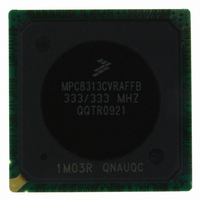
MPC8313CVRAFFB Freescale Semiconductor, MPC8313CVRAFFB Datasheet - Page 89
MPC8313CVRAFFB
Manufacturer Part Number
MPC8313CVRAFFB
Description
IC MPU POWERQUICC II PRO 516PBGA
Manufacturer
Freescale Semiconductor
Datasheet
1.MPC8313CZQAFFB.pdf
(100 pages)
Specifications of MPC8313CVRAFFB
Processor Type
MPC83xx PowerQUICC II Pro 32-Bit
Speed
333MHz
Voltage
0.95 V ~ 1.05 V
Mounting Type
Surface Mount
Package / Case
516-PBGA
Processor Series
MPC8xxx
Core
e300
Data Bus Width
32 bit
Development Tools By Supplier
MPC8313E-RDB
Maximum Clock Frequency
333 MHz
Operating Supply Voltage
- 0.3 V to + 1.26 V
Maximum Operating Temperature
+ 105 C
Mounting Style
SMD/SMT
I/o Voltage
2.5 V
Interface Type
I2C, SPI, UART
Minimum Operating Temperature
- 40 C
Program Memory Type
EEPROM/Flash
For Use With
MPC8313E-RDB - BOARD PROCESSOR
Lead Free Status / RoHS Status
Lead free / RoHS Compliant
Features
-
Lead Free Status / Rohs Status
Lead free / RoHS Compliant
Available stocks
Company
Part Number
Manufacturer
Quantity
Price
Company:

Part Number:
MPC8313CVRAFFB
Manufacturer:
FREESCAL
Quantity:
120
Company:
Part Number:
MPC8313CVRAFFB
Manufacturer:
Freescale Semiconductor
Quantity:
10 000
Part Number:
MPC8313CVRAFFB
Manufacturer:
FREESCALE
Quantity:
20 000


The SDAV
internal clock, the power supplied to the PLL is filtered using a circuit like the one shown in
For maximum effectiveness, the filter circuit should be placed as closely as possible to the SDAV
to ensure it filters out as much noise as possible. The ground connection should be near the SDAV
The 0.003-µF capacitor is closest to the ball, followed by the two 2.2-µF capacitors, and finally the 1-Ω
resistor to the board supply plane. The capacitors are connected from traces from SDAV
plane. Use ceramic chip capacitors with the highest possible self-resonant frequency. All traces should be
kept short, wide, and direct.
Note the following:
22.3
Due to large address and data buses, and high operating frequencies, the device can generate transient
power surges and high frequency noise in its power supply, especially while driving large capacitive loads.
This noise must be prevented from reaching other components in the MPC8313E system, and the
MPC8313E itself requires a clean, tightly regulated source of power. Therefore, it is recommended that
the system designer place at least one decoupling capacitor at each V
and LV
NV
minimize inductance. Capacitors may be placed directly under the device using a standard escape pattern.
Others may surround the part.
These capacitors should have a value of 0.01 or 0.1 µF. Only ceramic SMT (surface mount technology)
capacitors should be used to minimize lead inductance, preferably 0402 or 0603 sizes.
In addition, it is recommended that there be several bulk storage capacitors distributed around the PCB,
feeding the V
smaller chip capacitors. These bulk capacitors should have a low ESR (equivalent series resistance) rating
to ensure the quick response time necessary. They should also be connected to the power and ground
planes through two vias to minimize inductance. Suggested bulk capacitors—100 to 330 µF (AVX TPS
tantalum or Sanyo OSCON). However, customers should work directly with their power regulator vendor
for best values and types of bulk capacitors.
Freescale Semiconductor
DD
•
•
•
, GV
DDB
SDAV
Output signals on the SerDes interface are fed from the XPADV
sensitive transceiver analog circuits are on the XCOREV
Power: XPADV
750 mW.
Decoupling Recommendations
DD
DD
pin of the device. These decoupling capacitors should receive their power from separate V
DD
DD
, LV
signal provides power for the analog portions of the SerDes PLL. To ensure stability of the
, NV
should be a filtered version of XCOREV
XCOREV
DD
Note:
1. An 0805 sized capacitor is recommended for system initial bring-up.
MPC8313E PowerQUICC
DD
, LV
DD
, GV
DDA
DD
consumes less than 300 mW; XCOREV
Figure 59. SerDes PLL Power Supply Filter Circuit
DD
, LV
, LV
DDB
1.0 Ω
DD
, and VSS power planes in the PCB, utilizing short traces to
, LV
™
II Pro Processor Hardware Specifications, Rev. 3
DDA
2.2 µF
, and LV
1
DDB
DD
2.2 µF
.
planes, to enable quick recharging of the
1
DD
DD
supply.
DD
+ SDAV
DD
0.003 µF
, NV
power plane. Input signals and
DD
DD
SDAV
SDAV
, GV
consumes less than
System Design Information
DD
SS
DD
, LV
DD
to the ground
DD
Figure
, LV
DD
DD
DDA
59.
ball.
ball
DD
89
,
,
Related parts for MPC8313CVRAFFB
Image
Part Number
Description
Manufacturer
Datasheet
Request
R

Part Number:
Description:
Manufacturer:
Freescale Semiconductor, Inc
Datasheet:
Part Number:
Description:
Manufacturer:
Freescale Semiconductor, Inc
Datasheet:
Part Number:
Description:
Manufacturer:
Freescale Semiconductor, Inc
Datasheet:
Part Number:
Description:
Manufacturer:
Freescale Semiconductor, Inc
Datasheet:
Part Number:
Description:
Manufacturer:
Freescale Semiconductor, Inc
Datasheet:
Part Number:
Description:
Manufacturer:
Freescale Semiconductor, Inc
Datasheet:
Part Number:
Description:
Manufacturer:
Freescale Semiconductor, Inc
Datasheet:
Part Number:
Description:
Manufacturer:
Freescale Semiconductor, Inc
Datasheet:
Part Number:
Description:
Manufacturer:
Freescale Semiconductor, Inc
Datasheet:
Part Number:
Description:
Manufacturer:
Freescale Semiconductor, Inc
Datasheet:
Part Number:
Description:
Manufacturer:
Freescale Semiconductor, Inc
Datasheet:
Part Number:
Description:
Manufacturer:
Freescale Semiconductor, Inc
Datasheet:
Part Number:
Description:
Manufacturer:
Freescale Semiconductor, Inc
Datasheet:
Part Number:
Description:
Manufacturer:
Freescale Semiconductor, Inc
Datasheet:
Part Number:
Description:
Manufacturer:
Freescale Semiconductor, Inc
Datasheet: