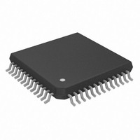
CS42436-DMZ Cirrus Logic Inc, CS42436-DMZ Datasheet - Page 37

CS42436-DMZ
Manufacturer Part Number
CS42436-DMZ
Description
IC CODEC 108DB 192KHZ 52-MQFP
Manufacturer
Cirrus Logic Inc
Type
Audio Codecr
Datasheet
1.CS42436-CMZ.pdf
(61 pages)
Specifications of CS42436-DMZ
Data Interface
Serial
Resolution (bits)
24 b
Number Of Adcs / Dacs
6 / 6
Sigma Delta
Yes
Dynamic Range, Adcs / Dacs (db) Typ
105 / 108 (Differential), 102 / 105 (Single-Ended)
Voltage - Supply, Analog
3.14 V ~ 5.25 V
Voltage - Supply, Digital
3.14 V ~ 3.47 V
Operating Temperature
-40°C ~ 105°C
Mounting Type
Surface Mount
Package / Case
52-MQFP, 52-PQFP
Audio Codec Type
Stereo
No. Of Adcs
6
No. Of Dacs
6
No. Of Input Channels
6
No. Of Output Channels
6
Adc / Dac Resolution
24bit
Sampling Rate
200kSPS
Ic Interface Type
I2C
Package
52MQFP
Adc/dac Resolution
24 Bit
Number Of Channels
6ADC /6 DAC
Number Of Dacs
6
Operating Supply Voltage
3.3|5 V
Lead Free Status / RoHS Status
Lead free / RoHS Compliant
Other names
598-1613
Available stocks
Company
Part Number
Manufacturer
Quantity
Price
Company:
Part Number:
CS42436-DMZ
Manufacturer:
CIRRUS
Quantity:
488
Company:
Part Number:
CS42436-DMZ
Manufacturer:
CRYSTAL
Quantity:
160
Company:
Part Number:
CS42436-DMZ
Manufacturer:
Cirrus Logic Inc
Quantity:
10 000
Company:
Part Number:
CS42436-DMZR
Manufacturer:
Cirrus Logic Inc
Quantity:
10 000
DS647F2
5.8
5.8.1
SCL
SDA
Recommended Power-Up Sequence
Since the read operation cannot set the MAP, an aborted write operation is used as a preamble. As shown
in
dition. The following pseudocode illustrates an aborted write operation followed by a read operation.
Send start condition.
Send 10010xx0 (chip address & write operation).
Receive acknowledge bit.
Send MAP byte, auto increment off.
Receive acknowledge bit.
Send stop condition, aborting write.
Send start condition.
Send 10010xx1(chip address & read operation).
Receive acknowledge bit.
Receive byte, contents of selected register.
Send acknowledge bit.
Send stop condition.
Setting the auto-increment bit in the MAP allows successive reads or writes of consecutive registers. Each
byte is separated by an acknowledge bit.
Hardware Mode
1. Hold RST low until the power supply, clocks and hardware control pins are stable. In this state, the
2. Bring RST high. The device will initially be in a low power state with VQ low.
3. The device will initiate the Hardware Mode power up sequence. All features will default to the
4. Following approximately 2000 sample periods, the device is initialized and ready for normal operation.
Note:
ware control pins.
START
Figure
control port is reset to its default settings and VQ will remain low.
Hardware Mode defaults as listed in
pins. VQ will quick-charge to approximately VA/2 and the analog output bias will clamp to VQ.
0
1
CHIP ADDRESS (WRITE)
1
0
During the Hardware Mode power-up sequence, there must be no transitions on any of the hard-
19, the write operation is aborted after the acknowledge for the MAP byte by sending a stop con-
0
2
1
3
0 AD1 AD0 0
4
5
6
7
ACK
8
Figure 19. Control Port Timing, I²C Read
9
INCR
10 11
6
5
MAP BYTE
12 13 14 15
4
3
2
1
Table 2 on page 26
16
0
ACK
STOP
17 18
START
19
1
20 21 22 23 24
CHIP ADDRESS (READ)
0
0
1
0 AD1 AD0 1
according to the Hardware Mode control
25
26 27 28
ACK
7
DATA
0
ACK
DATA +1
7
0
DATA + n
7
0
ACK
CS42436
NO
STOP
37


