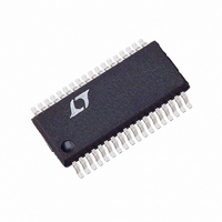
LTC4259ACGW-1#PBF Linear Technology, LTC4259ACGW-1#PBF Datasheet - Page 23

LTC4259ACGW-1#PBF
Manufacturer Part Number
LTC4259ACGW-1#PBF
Description
IC CTRLR POE QUAD AC DISC 36SSOP
Manufacturer
Linear Technology
Datasheet
1.LTC4259ACGW-1PBF.pdf
(32 pages)
Specifications of LTC4259ACGW-1#PBF
Controller Type
Power over Ethernet Controller (POE)
Interface
I²C
Voltage - Supply
3 V ~ 4 V
Current - Supply
2.5mA
Operating Temperature
0°C ~ 70°C
Mounting Type
Surface Mount
Package / Case
36-SSOP
Linear Misc Type
Negative Voltage
Family Name
LTC4259A
Package Type
SSOP
Operating Supply Voltage (min)
-48V
Operating Supply Voltage (max)
-57V
Operating Temperature (min)
0C
Operating Temperature (max)
70C
Operating Temperature Classification
Commercial
Mounting
Surface Mount
Pin Count
36
Lead Free Status / RoHS Status
Lead free / RoHS Compliant
Available stocks
Company
Part Number
Manufacturer
Quantity
Price
APPLICATIO S I FOR ATIO
Assumimg that f
0.05µF of cable capacitance gives a port impedance of 10k
at 100Hz. The PD AC signature resistance is about 25k.
Connecting a PD with the maximum allowed resistance of
26.25k brings the connection impedance to about 8k. The
presence of a PD only makes a 20% reduction in the port
impedance requiring the AC disconnect circuitry to be
quite sensitive. When the OSCIN pin is driven with a sine
wave, the LTC4259A-1 is able to distinguish between
capacitive impedance and resistive impedance on the
Power over Ethernet connection. AC disconnect is reliable
for cable capacitance up to about 0.2µF, nearly an order of
magnitude greater than worst case for a long CAT-3 or
CAT-5 cable.
OSCIN Input and Oscillator Requirements
AC disconnect depends on an external oscillator source
applied to the OSCIN pin. The LTC4259A-1 measures port
impedance by applying an amplified version of the OSCIN
signal to the port’s DETECT pin (see Figure 18). The
oscillator should be well-controlled because errors in this
signal become errors in the measured port impedance. As
shown in Figure 19, the load being sensed by AC discon-
nect has a resistive and a large reactive component.
Current through the PD’s signature resistor depends on
the amplitude of the AC signal while current into the
capacitors depends on the slew rated: I = C • dV/dt.
Consequently, the LTC4259A-1 is sensitive to the ampli-
tude and slew rate of the OSCIN signal, but is more
tolerant of frequency and offset errors. Internal limits
prevent the LTC4259A-1 from being adversely affected by
OSCIN signals with excessive amplitude.
There are many ways to build oscillators with controlled
amplitudes and slew rates, especially since the frequency
of the oscillator does not have to be well-controlled.
Contact the LTC Applications department for oscillator
circuits.
As alluded to previously, AC disconnect is complicated
and redesigning for different component sizes is a difficult
task. For optimum performance, use the recommended
component values and drive OSCIN with a 100Hz 2V
1.2V offset sine wave. Keep in mind that the IEEE 802.3af
specification places upper limits of 100V/ms on the slew
OSCIN
U
is 100Hz, the 0.1µF of C
U
W
U
PSE
plus
P-P
,
rate and 500Hz on the frequency of the AC signal at the
port. Voltage gain, A
creases the slew rate by the voltage gain. Since A
a maximum absolute value of 3.3V/V (±3V typ), the slew
rate at the OSCIN pin must be less than 30V/ms. A slew
rate around 0.6V/ms at OSCIN will work with the recom-
mended values of C
The LTC4259A-1’s OSCIN input amplifier will accept sig-
nals between DGND – 0.3V and V
has a gain of –1 and is referenced to 1.2V above DGND. An
OSCIN voltage greater than 2.2V will cause the amplifier’s
output to clip against DGND. Clipping will not affect the
performance of AC disconnect until the clipping becomes
so severe that even the midrange (where the controlled
slew rate occurs) of the signal is clipped. Keep the midrange
or average voltage of the OSCIN signal between 0.9V and
1.5V to avoid severe clipping. OSCIN signals below DGND
can interact with the ESD protection circuitry on the pin
and are not recommended. Also, meeting the IEEE 802.3af
specification for maximum AC amplitude on the port just
after the PD is removed depends on the OSCIN input peak-
to-peak amplitude. Clipping by LTC4259A-1’s OSCIN in-
put circuitry will generally ensure that this specification is
not exceeded. Note that under normal operation, the AC
disconnect output on the DETECT n pin will have an ampli-
tude near 6V peak-to-peak. The combination of R
and C
tude is seen at the port when the port is powered and the
PD has just been removed. When the PD is still connected
there will be almost no AC signal at the port.
The LTC4259A-1 monitors Pin 36 for the presence of an
oscillating signal. If no signal is present and the Osc Fail
Mask bit is set, then Osc Fail (bit 1 of the Supply Event
register) is set, triggering an interrupt. As the LTC4259A-
1’s AC disconnect circuitry self-checks the OSCIN signal,
the Osc Fail bit is intended as a fault indicator to alert the
PSE host controller. The Osc Fail bit has no effect beyond
triggering the interrupt. A clear Osc Fail bit indicates that
the OSCIN signal goes below 0.6V and above 1.8V at least
once every 250ms. It does not necessarily guarantee that
AC disconnect will function properly. However, AC discon-
nect itself is a more thorough test of the OSCIN signal.
When the OSCIN signal is either absent or corrupted,
PSE
attenuate the signal so roughly half this ampli-
DET
VACD
, R
, from OSCIN to DETECT n in-
DET
and C
LTC4259A-1
DD
+ 0.5V. This amplifier
PSE
.
DET
VACD
23
, C
4259a1fa
has
DET


