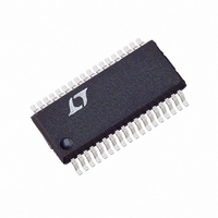
LTC4259ACGW-1#PBF Linear Technology, LTC4259ACGW-1#PBF Datasheet - Page 8

LTC4259ACGW-1#PBF
Manufacturer Part Number
LTC4259ACGW-1#PBF
Description
IC CTRLR POE QUAD AC DISC 36SSOP
Manufacturer
Linear Technology
Datasheet
1.LTC4259ACGW-1PBF.pdf
(32 pages)
Specifications of LTC4259ACGW-1#PBF
Controller Type
Power over Ethernet Controller (POE)
Interface
I²C
Voltage - Supply
3 V ~ 4 V
Current - Supply
2.5mA
Operating Temperature
0°C ~ 70°C
Mounting Type
Surface Mount
Package / Case
36-SSOP
Linear Misc Type
Negative Voltage
Family Name
LTC4259A
Package Type
SSOP
Operating Supply Voltage (min)
-48V
Operating Supply Voltage (max)
-57V
Operating Temperature (min)
0C
Operating Temperature (max)
70C
Operating Temperature Classification
Commercial
Mounting
Surface Mount
Pin Count
36
Lead Free Status / RoHS Status
Lead free / RoHS Compliant
Available stocks
Company
Part Number
Manufacturer
Quantity
Price
PI FU CTIO S
LTC4259A-1
RESET (Pin 1): Chip Reset, Active Low. When the RESET
pin is low, the LTC4259A-1 is held inactive with all ports
off and all internal registers reset to their power-up states.
When RESET is pulled high, the LTC4259A-1 begins
normal operation. RESET can be connected to an external
capacitor or RC network to provide a power turn-on delay.
Internal filtering of the RESET pin prevents glitches less
than 1µs wide from resetting the LTC4259A-1. Pull RESET
high with ≤10k or tie to V
BYP (Pin 2): Bypass Output. The BYP pin is used to
connect the internally generated – 20V supply to an exter-
nal 0.1µF bypass capacitor. Use a 100V rated 0.1µF, X7R
capacitor. Do not connect the BYP pin to any other external
circuitry.
INT (Pin 3): Interrupt Output, Open Drain. INT will pull low
when any one of several events occur in the LTC4259A-1.
It will return to a high impedance state when bits 6 or 7 are
set in the Reset PB register (1Ah). The INT signal can be
used to generate an interrupt to the host processor,
eliminating the need for continuous software polling.
Individual INT events can be disabled using the Int Mask
register (01h). See Register Functions and Applications
Information for more information. The INT pin is only
updated between I
SCL (Pin 4): Serial Clock Input. High impedance clock
input for the I
be connected directly to the I
SDAOUT (Pin 5): Serial Data Output, Open Drain Data
Output for the I
uses two pins to implement the bidirectional SDA function
to simplify optoisolation of the I
dard bidirectional SDA pin, tie SDAOUT and SDAIN together.
See Applications Information for more information.
SDAIN (Pin 6): Serial Data Input. High impedance data input
for the I
pins to implement the bidirectional SDA function to sim-
plify optoisolation of the I
bidirectional SDA pin, tie SDAOUT and SDAIN together.
See Applications Information for more information.
AD3 (Pin 7): Address Bit 3. Tie the address pins high or low
to set the I
8
U
2
C serial interface bus. The LTC4259A-1 uses two
U
2
C serial address to which the LTC4259A-1
2
C serial interface bus. The SCL pin should
2
C Serial Interface Bus. The LTC4259A-1
2
C transactions.
U
2
DD
C bus. To implement a standard
.
2
2
C SCL bus line.
C bus. To implement a stan-
responds. This address will be (010A
high or low with ≤10k or tie to V
AD2 (Pin 8): Address Bit 2. See AD3.
AD1 (Pin 9): Address Bit 1. See AD3.
AD0 (Pin 10): Address Bit 0. See AD3.
DETECT1 (Pin 11): Detect Sense, Port 1. The LTC4259A-
1 Powered Device (PD) detection, classification and AC
disconnect hardware monitors port 1 with this pin. Con-
nect DETECT1 to the output port via a 0.47µF 100V X7R
capacitor in series with a 1k resistor, both in parallel with
a low leakage diode (see Figure 1). The resistor and
capacitor may be eliminated if AC disconnect is not used.
If the port is unused, the DETECT1 pin can be tied to DGND
or allowed to float.
DETECT2 (Pin 12): Detection Sense, Port 2. See DETECT1.
DETECT3 (Pin 13): Detection Sense, Port 3. See DETECT1.
DETECT4 (Pin 14): Detection Sense, Port 4. See DETECT1.
DGND (Pin 15): Digital Ground. DGND should be con-
nected to the return from the 3.3V supply. DGND and
AGND should be tied together.
V
power supply relative to DGND. V
DGND near the LTC4259A-1 with at least a 0.1µF capaci-
tor.
SHDN1 (Pin 17): Shutdown Port 1, Active Low. When
pulled low, SHDN1 shuts down port 1, regardless of the
state of the internal registers. Pulling SHDN1 low is
equivalent to setting the Reset Port 1 bit in the Reset
Pushbutton register (1Ah). Internal filtering of the SHDN1
pin prevents glitches less than 1µs wide from reseting the
LTC4259A-1. Pull SHDN1 high with ≤10k or tie to V
SHDN2 (Pin 18): Shutdown Port 2, Active Low. See
SHDN1.
SHDN3 (Pin 19): Shutdown Port 3, Active Low. See
SHDN1.
SHDN4 (Pin 20): Shutdown Port 4, Active Low. See
SHDN1.
DD
(Pin 16): Logic Power Supply. Connect to a 3.3V
DD
DD
or DGND.
must be bypassed to
3
A
2
A
1
A
0
)
b
. Pull AD3
4259a1fa
DD
.


