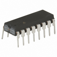
HIN232CP Intersil, HIN232CP Datasheet - Page 11

HIN232CP
Manufacturer Part Number
HIN232CP
Description
IC TXRX RS-232 5V 16-PDIP
Manufacturer
Intersil
Type
Transceiverr
Datasheet
1.HIN232CBZ.pdf
(21 pages)
Specifications of HIN232CP
Number Of Drivers/receivers
2/2
Protocol
RS232
Voltage - Supply
4.5 V ~ 5.5 V
Mounting Type
Through Hole
Package / Case
16-DIP (0.300", 7.62mm)
Lead Free Status / RoHS Status
Contains lead / RoHS non-compliant
Available stocks
Company
Part Number
Manufacturer
Quantity
Price
Company:
Part Number:
HIN232CP
Manufacturer:
INTERSIL
Quantity:
5 380
Company:
Part Number:
HIN232CP
Manufacturer:
INTERSIL
Quantity:
5 380
Company:
Part Number:
HIN232CP
Manufacturer:
Intersil
Quantity:
156
Part Number:
HIN232CP
Manufacturer:
INTERSIL
Quantity:
20 000
Part Number:
HIN232CPA
Manufacturer:
HIN
Quantity:
20 000
Company:
Part Number:
HIN232CPE
Manufacturer:
FREESCALE
Quantity:
13
Company:
Part Number:
HIN232CPZ
Manufacturer:
TI
Quantity:
2 500
Part Number:
HIN232CPZ
Manufacturer:
INTERSIL
Quantity:
20 000
Transmitters
The transmitters are TTL/CMOS compatible inverters which
translate the inputs to RS-232 outputs. The input logic threshold
is about 26% of V
input results in a voltage of between -5V and V- at the output,
and a logic 0 results in a voltage between +5V and (V+ -0.6V).
Each transmitter input has an internal 400kΩ pullup resistor so
any unused input can be left unconnected and its output
remains in its low state. The output voltage swing meets the
RS-232C specifications of ±5V minimum with the worst case
conditions of: all transmitters driving 3kΩ minimum load
impedance, V
temperature. The transmitters have an internally limited output
slew rate which is less than 30V/µs. The outputs are short
circuit protected and can be shorted to ground indefinitely. The
powered down output impedance is a minimum of 300Ω with
±2V applied to the outputs and V
GND < T
T
V
XIN
XIN
V+
CC
V-
CC
< V
CC
= 4.5V, and maximum allowable operating
CC
FIGURE 2. TRANSMITTER
, or 1.3V for V
400kΩ
HIN232, HIN236, HIN237, HIN238, HIN239, HIN240, HIN241
11
CC
AVERAGE PROPAGATION DELAY =
CC
= 0V.
= 5V. A logic 1 at the
300Ω
FIGURE 4. PROPAGATION DELAY DEFINITION
T
R
V- < V
OR
OUT
OUT
R
T
OR
IN
IN
T
TOUT
OUT
t
PHL
< V+
t
PHL +
t
PLH
Receivers
The receiver inputs accept up to ±30V while presenting the
required 3kΩ to 7kΩ input impedance even if the power is off
(V
1.3V which is within the ±3V limits, known as the transition
region, of the RS-232 specifications. The receiver output is
0V to V
greater than 2.4V and high whenever the input is floating or
driven between +0.8V and -30V. The receivers feature 0.5V
hysteresis to improve noise rejection. The receiver Enable
line EN, when set to logic “1”, (HIN236, HIN239, HIN240,
and HIN241) disables the receiver outputs, placing them in
the high impedance mode. The receiver outputs are also
placed in the high impedance state when in shutdown mode.
2
CC
t
PLH
= 0V). The receivers have a typical input threshold of
CC
-30V < R
. The output will be low whenever the input is
XIN
R
GND
V
XIN
CC
< +30V
V
V
OL
OL
FIGURE 3. RECEIVER
5kΩ
GND < V
R
ROUT
OUT
September 26, 2008
< V
CC
FN3138.16


