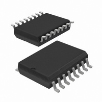
MC145406D,518 NXP Semiconductors, MC145406D,518 Datasheet - Page 2

MC145406D,518
Manufacturer Part Number
MC145406D,518
Description
IC DRIVER/RECEIVER TRIPLE 16SOIC
Manufacturer
NXP Semiconductors
Type
Transceiverr
Datasheet
1.MC145406N602.pdf
(5 pages)
Specifications of MC145406D,518
Number Of Drivers/receivers
3/3
Protocol
RS232
Voltage - Supply
4.5 V ~ 5.5 V
Mounting Type
Surface Mount
Package / Case
16-SOIC (0.300", 7.5mm Width)
Logic Family
MC145
Logic Type
Driver/Receiver
Maximum Operating Temperature
+ 70 C
Mounting Style
SMD/SMT
Interface
EIA/TIA- 232- D. V.28
Maximum Power Dissipation
1 W
Minimum Operating Temperature
0 C
Number Of Lines (input / Output)
6 / 6
Propagation Delay Time
500 ns
Lead Free Status / RoHS Status
Lead free / RoHS Compliant
Other names
568-1193-2
935024380518
MC145406D,623
MC145406D-T
935024380518
MC145406D,623
MC145406D-T
Philips Semiconductors Linear Products
BLOCK DIAGRAM
August 31, 1994
11, 13, 15
10, 12, 14
EIA-232-D/V.28 driver/receiver
2, 4, 6
3, 5, 7
PIN #
16
1
8
9
DO1, DO2, DO3
RX
TX1, TX2, TX3
DI1, DI2, DI3
SYMBOL
1
, RX
GND
V
V
V
DD
SS
CC
2
RX
TX
, RX
3
300
Positive power supply. The most positive power supply pin, which is typically 5 to 12 volts.
Negative power supply. The most negative power supply pin, which is typically -5 to -12 volts.
Digital power supply. The digital supply pin, which is connected to the logic power supply (maximum +5.5V).
Ground. Ground return pin is typically connected to the signal ground pin of the EIA-232-D connector (Pin 7)
as well as to the logic power supply ground.
Receive Data Input. These are the EIA-232-D receive signal inputs whose voltages can range from +25 to
-25V. A voltage between +3 and +25 is decoded as a space and causes the corresponding DO pin to swing
to ground (0V); a voltage between -3 and -25V is decoded as a mark and causes the DO pin to swing up to V
The actual turn-on input switchpoint is typically biased at 1.8V above ground, and includes 800mV of hysteresis
for noise rejection. The nominal input impedance is 5k . An open or grounded input pin is interpreted as a mark,
forcing the DO pin to V
Data Output. These are the receiver digital output pins, which swing from V
pin causes DO to produce a logic zero; a mark produces a logic one. Each output pin is capable of driving one
LSTTL input load.
Data Input. These are the high-impedance digital input pins to the drivers. TTL compatibility is accomplished
by biasing the input switchpoint at 1.4V above ground. However, 5V CMOS compatibility is maintained as well.
Input voltage levels on these pins must be between V
Transmit Data Output. These are the EIA-232-D transmit signal output pins, which swing toward V
A logic one at a DI input causes the corresponding TX output to swing toward V
output to swing toward V
load). Output slew rates are limited to a maximum of 30V/ s. When the MC145406 is off (V
= GND), the minimum output impedance is 300 .
5.4k
V
V
SS
DD
15k
CC
DD
V
.
SS
(the output voltages will be slightly less than V
RECEIVER
DRIVER
468
LEVEL
SHIFT
+
–
PIN DESCRIPTION
V
CC
HYSTERESIS
CC
V
CC
and GND.
+
–
1.8V
1.0V
1.4V
V
CC
DD
or V
CC
SS
to GND. A space on the RX
SS
DO
depending upon the output
DI
. A logic zero causes the
MC145406
Product specification
DD
= V
DD
SS
and V
= V
CC
SS
CC
.
.


