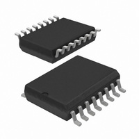
MC145406D,518 NXP Semiconductors, MC145406D,518 Datasheet - Page 3

MC145406D,518
Manufacturer Part Number
MC145406D,518
Description
IC DRIVER/RECEIVER TRIPLE 16SOIC
Manufacturer
NXP Semiconductors
Type
Transceiverr
Datasheet
1.MC145406N602.pdf
(5 pages)
Specifications of MC145406D,518
Number Of Drivers/receivers
3/3
Protocol
RS232
Voltage - Supply
4.5 V ~ 5.5 V
Mounting Type
Surface Mount
Package / Case
16-SOIC (0.300", 7.5mm Width)
Logic Family
MC145
Logic Type
Driver/Receiver
Maximum Operating Temperature
+ 70 C
Mounting Style
SMD/SMT
Interface
EIA/TIA- 232- D. V.28
Maximum Power Dissipation
1 W
Minimum Operating Temperature
0 C
Number Of Lines (input / Output)
6 / 6
Propagation Delay Time
500 ns
Lead Free Status / RoHS Status
Lead free / RoHS Compliant
Other names
568-1193-2
935024380518
MC145406D,623
MC145406D-T
935024380518
MC145406D,623
MC145406D-T
1. This is the range of input voltages as specified by EIA-232-D to cause a receiver to be in the high or low logic state.
Philips Semiconductors Linear Products
ABSOLUTE MAXIMUM RATINGS
NOTE: This device contains protection circuitry to protect the inputs against damage due to high static voltages or electric fields; however, it is
advised that normal precautions be taken to avoid application of any voltage higher than maximum rated voltages to this high impedance circuit.
For proper operation, it is recommended that the voltages at the DI and DO pins be constrained to the range GND < V
< V
must always be tied to an appropriate logic voltage level (e.g., GND or V
DC ELECTRICAL CHARACTERISTICS
Typical values are at T
RECEIVER ELECTRICAL CHARACTERISTICS
Typical values are at T
NOTE:
August 31, 1994
SYMBOL
SYMBOL
DC supply voltage
Quiescent supply current (outputs unloaded, inputs low)
V
SYMBOL
SYMBOL
EIA-232-D/V.28 driver/receiver
ON
CC
V
V
V
V
I
I
I
SYMBOL
V
V
V
V
DD
CC
R
SS
DD
CC
SS
OFF
-V
. Also, the voltage at the RX pin should be constrained to +25V, and TX should be constrained to V
ON
OH
OL
OL
IN
T
V
V
V
V
P
T
OFF
STG
CC
DD
JA
SS
IR
A
D
Input turn-on threshold
Input turn-off threshold
Input threshold hysteresis
Input resistance
High level output voltage
V
Low level output voltage
Low level output voltage
V
V
V
RX1-3
RX1-3
RX1-3
RX1-3
Supply voltage
Supply voltage
Supply voltage
Input voltage range
DC current per pin
Power dissipation (package)
Operating temperature range
Storage temperature range
Thermal impedance
= -3V to (V
= +3V to (V
= +3V to (V
= +3V to (V
A
A
= 0 to 70 C; GND = 0V, unless otherwise specified.
= 0 to 70 C; GND = 0V; V
PARAMETER
PARAMETER
PARAMETER
PARAMETER
RX
DI
1-3
SS
DD
DD
DD
1-3
-15V)
inputs
+15V)
+15V)
+15V)
inputs
1
1
1
1
PARAMETER
N package
D package
RX
RX
RX
RX
DO
DO
DO
1-3
1-3
1-3
1-3
1-3
1-3
1-3
DD
= +5 to +12V; V
(V
V
V
DO1-3
SS
DO1-3
I
I
I
I
I
OL
OH
OL
OL
OH
-15V) < V
SS
469
TEST CONDITIONS
TEST CONDITIONS
TEST CONDITIONS
TEST CONDITIONS
= +20 A, V
= +2mA, V
= +4mA, V
= -20 A, V
= -1mA, V
CC
= -5 to -12V; V
V
= V
= V
CC
V
V
V
for DI, and V
OH
OL
DD
SS
CC
= 5.0V +5%
RX1-3
, V
, V
= +12V
= -12V
= +5V
CC
CC
CC
CC
CC
CC
CC
< (V
= 5.0V +5%
= 5.0V +5%
= +5.0V
= +5.0V
= +5.0V
= +5.0V
= +5.0V
CC
SS
DD
= +5V +5%, unless otherwise specified.
+15V)
or V
(V
DD
SS
-0.5 to (V
for RX).
- 15) to (V
-0.5 to +13.5
+0.5 to -13.5
-0.5 to +6.0
-65 to +150
RATING
0 to +70
+100
105
1.0
80
MIN
1.35
0.75
MIN
-4.5
4.5
4.5
0.6
3.0
4.9
3.8
SS
CC
< V
+ 0.5)
DD
TX1-3
+ 15)
-5 to -12
LIMITS
LIMITS
5 to 12
0.005
TYP
TYP
1.80
1.00
0.15
280
260
5.0
0.8
5.0
5.0
4.4
0.3
20
< V
DI
< V
DD
MC145406
Product specification
DD
. Unused inputs
and GND < V
MAX
-13.2
MAX
13.2
2.35
1.25
400
600
450
5.5
7.0
0.1
0.5
0.7
UNITS
mA
C/W
W
V
V
V
V
C
C
UNITS
UNITS
UNITS
UNITS
k
V
V
V
V
V
V
V
V
V
V
A
A
A
DO


