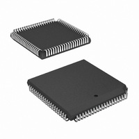
HSP43220JC-25Z Intersil, HSP43220JC-25Z Datasheet

HSP43220JC-25Z
Specifications of HSP43220JC-25Z
Available stocks
Related parts for HSP43220JC-25Z
HSP43220JC-25Z Summary of contents
Page 1
... PART PART NUMBER MARKING HSP43220JC-25 HSP43220JC-25 HSP43220JC-25Z HSP43220JC-25Z HSP43220JC-33 HSP43220JC-33 HSP43220JC-33Z HSP43220JC-33Z NOTE: These Intersil Pb-free plastic packaged products employ special Pb- free material sets, molding compounds/die attach materials, and 100% matte tin plate plus anneal (e3 termination finish, which is RoHS compliant and compatible with both SnPb and Pb-free soldering operations) ...
Page 2
Block Diagram INPUT CLOCK DATA INPUT CONTROL AND COEFFICIENTS Pinout STARTOUT V CC STARTIN ASTARTIN RESET C_BUS 15 C_BUS 14 C_BUS 13 C_BUS 12 C_BUS 11 C_BUS 10 C_BUS GND C_BUS 8 C_BUS ...
Page 3
Pin Description (Continued) NAME TYPE DATA_IN0-15 I Input Data Bus. This bus is used to provide the 16-bit input data to the HSP43220. The data must be provided in a synchronous fashion, and is latched on the rising edge of ...
Page 4
Integrator Section The data from the shifter goes to the Integrator section. This is a cascade of 5 integrator (or accumulator) stages, which implement a low pass filter. Each accumulator is implemented as an adder followed by a register in ...
Page 5
COMB_EN5 COMB_EN4 FROM DECIMATION REGISTER RESET RESET REG B A-B REG CK_DEC Comb Filter Section The output of the Decimation Register is passed to the Comb Filter Section. The Comb section consists of 5 cascaded Comb filters ...
Page 6
DDF Control Registers F_Register ( F_OAD F_BYP F_ESYM F_DRATE FA0 FB0 ES0 HSP43220 F_TAPS 10 9 ...
Page 7
DDF Control Registers (Continued) FC_Register ( C19 C18 C17 C16 C15 C14 C13 C12 C11 C10 HSP43220 F_CF C9 C8 ...
Page 8
DDF Control Registers (Continued) H_Register 1 ( RESERVED F_DIS F_CLA H_BYP FD0 FC0 HB0 HSP43220 H_DRATE ...
Page 9
DDF Control Registers (Continued) H_Register 2 ( RESERVED Start Logic The Start Logic generates a start signal that is used internally to synchronously start ...
Page 10
... HDF does not apply). In the “Operational Section” on page 12 under the Design Considerations, there is a table that shows the trade-offs of these parameters. In addition, Intersil provides a software package called DECI MATE™ which designs the DDF filter from System specifications. ...
Page 11
FIR Output The 40 most significant bits of the accumulator are latched into the output register. The lower 3 bits are not brought to the output. The 40 bits out of the output register are selected to be output by ...
Page 12
F_BYP = 0 OUT_SELH = F_BYP OUT_SELH OUT_ENX DATA_OUT16- ...
Page 13
Multi-Chip Start Configurations Since there are two methods to start-up the DDF, there are also two configurations that can be used to start-up multiple chips. The first method is shown in Figure 12. The timing of the STARTOUT circuitry starts ...
Page 14
SAMPLED INPUT DATA 0 FIR_CK SPEED GRADE (MHz) CK_IN MIN NOTE: Filter not realizable. 14 ...
Page 15
... DECIMATE Intersil provides a development system which assists the design engineer to utilizing this filter. The DECIMATE software package provides the user with both filter design and simulation environments for filter evaluation and design. These tools are integrated within one standard DSP CAD environment, The Athena Group's Monarch Professional DSP Software package ...
Page 16
HSP43220 FIGURE 15. DECIMATE DESIGN MODULE SCREENS 16 FN2486.10 October 10, 2008 ...
Page 17
... Thermal Resistance (Typical, Note 1) +0.5V PLCC Package Maximum Storage Temperature Range . . . . . . . . . .-65°C to +150°C Maximum Junction Temperature PLCC Package +150°C Pb-Free Reflow Profile .see link below http://www.intersil.com/pbfree/Pb-FreeReflow.asp Die Characteristics Component Count . . . . . . . . . . . . . . . . . . . . . . . 193,000 Transistors SYMBOL TEST CONDITIONS 5.25V IH ...
Page 18
AC Electrical Specifications V tested at +25°C, unless otherwise specified. Temperature limits established by characterization and are not production tested. PARAMETER Input Clock Frequency FIR Clock Frequency Input Clock Period FIR Clock Period Clock Pulse Width Low Clock Pulse Width ...
Page 19
AC Test Load Circuit SWITCH S1 OPEN FOR I NOTE: Test head capacitance. Timing Waveforms t SET t CLK_IN HOLD DATA_IN FIGURE 16A. t AST ASTARTIN CK_IN STARTOUT CK_IN t STIC STARTIN t HOLD DATA_IN FIGURE 17A. 19 HSP43220 S ...
Page 20
Timing Waveforms (Continued) FIR_CK t FIRDR DATA_RDY t DRPWL t FIRDV DATA_OUT PREVIOUS OUTPUT FIGURE 18A. 2.0V DATA_OUT 0-d23 t r FIGURE 18C. 20 HSP43220 t FIRDR DATA_OUT 16-23 OUT_SELH CURRENT OUTPUT OUT_ENP OUT_ENX DATA_OUT 0. FIGURE 18. ...
Page 21
... Accordingly, the reader is cautioned to verify that data sheets are current before placing orders. Information furnished by Intersil is believed to be accurate and reliable. However, no responsibility is assumed by Intersil or its subsidiaries for its use; nor for any infringements of patents or other rights of third parties which may result from its use ...


