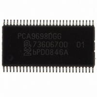
PCA9698DGG,512 NXP Semiconductors, PCA9698DGG,512 Datasheet - Page 12

PCA9698DGG,512
Manufacturer Part Number
PCA9698DGG,512
Description
IC I/O EXPANDER I2C 40B 56TSSOP
Manufacturer
NXP Semiconductors
Datasheet
1.PCA9698BS118.pdf
(48 pages)
Specifications of PCA9698DGG,512
Package / Case
56-TSSOP
Interface
I²C
Number Of I /o
40
Interrupt Output
Yes
Frequency - Clock
1MHz
Voltage - Supply
2.3 V ~ 5.5 V
Operating Temperature
-40°C ~ 85°C
Mounting Type
Surface Mount
Includes
POR
Logic Family
PCA9698
Number Of Lines (input / Output)
40.0 / 40.0
Operating Supply Voltage
2.3 V to 5.5 V
Power Dissipation
500 mW
Operating Temperature Range
- 40 C to + 85 C
Input Voltage
5.5 V
Logic Type
I2C Bus
Maximum Clock Frequency
1 MHz
Mounting Style
SMD/SMT
Number Of Input Lines
40.0
Number Of Output Lines
40.0
Output Current
50 mA
Output Voltage
5.5 V
Lead Free Status / RoHS Status
Lead free / RoHS Compliant
For Use With
OM6281 - DAUGHTER CARD PCA9698 FOR OM6275
Lead Free Status / Rohs Status
Lead free / RoHS Compliant
Other names
568-3241-5
935278614512
PCA9698DGG
935278614512
PCA9698DGG
Available stocks
Company
Part Number
Manufacturer
Quantity
Price
Part Number:
PCA9698DGG,512
Manufacturer:
NXP/恩智浦
Quantity:
20 000
NXP Semiconductors
Table 6.
Legend: * default value.
Table 7.
Legend: * default value.
PCA9698
Product data sheet
Address
10h
11h
12h
13h
14h
Address
18h
19h
1Ah
1Bh
1Ch
PI0 to PI4 - Polarity Inversion registers (address 10h to 14h) bit description
IOC0 to IOC4 - I/O Configuration registers (address 18h to 1Ch) bit description
Register
PI0
PI1
PI2
PI3
PI4
Register
IOC0
IOC1
IOC2
IOC3
IOC4
7.4.3 PI0 to PI4 - Polarity Inversion registers
7.4.4 IOC0 to IOC4 - I/O Configuration registers
These registers allow inversion of the polarity of the corresponding Input Port register.
Where ‘x’ refers to the bank number (0 to 4); ‘y’ refers to the bit number (0 to 7).
These registers configure the direction of the I/O pins.
Where ‘x’ refers to the bank number (0 to 4); ‘y’ refers to the bit number (0 to 7).
Px[y] = 0: The corresponding Input Port register data polarity is retained.
Px[y] = 1: The corresponding Input Port register data polarity is inverted.
Cx[y] = 0: The corresponding port pin is an output.
Cx[y] = 1: The corresponding port pin is an input.
Bit
7 to 0
7 to 0
7 to 0
7 to 0
7 to 0
Bit
7 to 0
7 to 0
7 to 0
7 to 0
7 to 0
All information provided in this document is subject to legal disclaimers.
Symbol
P0[7:0]
P1[7:0]
P2[7:0]
P3[7:0]
P4[7:0]
Symbol
C0[7:0]
C1[7:0]
C2[7:0]
C3[7:0]
C4[7:0]
40-bit Fm+ I
Rev. 3 — 3 August 2010
Access
R/W
R/W
R/W
R/W
R/W
Access
R/W
R/W
R/W
R/W
R/W
2
C-bus advanced I/O port with RESET, OE and INT
Value
0000 0000*
0000 0000*
0000 0000*
0000 0000*
0000 0000*
Value
1111 1111*
1111 1111*
1111 1111*
1111 1111*
1111 1111*
Description
Polarity Inversion register bank 0
Polarity Inversion register bank 1
Polarity Inversion register bank 2
Polarity Inversion register bank 3
Polarity Inversion register bank 4
Description
I/O Configuration register bank 0
I/O Configuration register bank 1
I/O Configuration register bank 2
I/O Configuration register bank 3
I/O Configuration register bank 4
PCA9698
© NXP B.V. 2010. All rights reserved.
12 of 48


