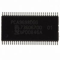
PCA9698DGG,512 NXP Semiconductors, PCA9698DGG,512 Datasheet - Page 17

PCA9698DGG,512
Manufacturer Part Number
PCA9698DGG,512
Description
IC I/O EXPANDER I2C 40B 56TSSOP
Manufacturer
NXP Semiconductors
Datasheet
1.PCA9698BS118.pdf
(48 pages)
Specifications of PCA9698DGG,512
Package / Case
56-TSSOP
Interface
I²C
Number Of I /o
40
Interrupt Output
Yes
Frequency - Clock
1MHz
Voltage - Supply
2.3 V ~ 5.5 V
Operating Temperature
-40°C ~ 85°C
Mounting Type
Surface Mount
Includes
POR
Logic Family
PCA9698
Number Of Lines (input / Output)
40.0 / 40.0
Operating Supply Voltage
2.3 V to 5.5 V
Power Dissipation
500 mW
Operating Temperature Range
- 40 C to + 85 C
Input Voltage
5.5 V
Logic Type
I2C Bus
Maximum Clock Frequency
1 MHz
Mounting Style
SMD/SMT
Number Of Input Lines
40.0
Number Of Output Lines
40.0
Output Current
50 mA
Output Voltage
5.5 V
Lead Free Status / RoHS Status
Lead free / RoHS Compliant
For Use With
OM6281 - DAUGHTER CARD PCA9698 FOR OM6275
Lead Free Status / Rohs Status
Lead free / RoHS Compliant
Other names
568-3241-5
935278614512
PCA9698DGG
935278614512
PCA9698DGG
Available stocks
Company
Part Number
Manufacturer
Quantity
Price
Part Number:
PCA9698DGG,512
Manufacturer:
NXP/恩智浦
Quantity:
20 000
NXP Semiconductors
PCA9698
Product data sheet
7.6 GPIO All Call
7.7 Output state change on ACK or STOP
A ‘GPIO All Call’ command allows the programming of multiple advanced GPIOs with
different I
when the master needs to send the same instruction to several devices. To respond to
such a command and sequence, the PCA9698 needs to have its IOAC bit (register 2Ah,
bit 3) set to 1. Devices that have this bit set to 0 do not participate in any ‘GPIO All Call’
sequence.
The ‘GPIO All Call’ command can be performed only for a write operation and cannot be
used in conjunction with a read operation.
If the master initiates a ‘GPIO All Call’ sequence with a Read command, none of the slave
devices acknowledge.
State change of the I/Os programmed as outputs can be done either:
Change of the outputs at the STOP command allows synchronizing of all the programmed
banks in a single device, and also allows synchronizing outputs of more than one
PCA9698.
Example 1: Only one PCA9698 is used on the I
at the same time.
Example 2: More than one PCA9698 is used on the I
change at the same time.
•
•
•
•
•
•
•
•
•
•
•
•
•
Master initiates a command sequence with the START command, the ‘GPIO All Call’
command associated with a Write command: Start − 1101 110 + Write
All the devices that are programmed to respond to this command will acknowledge
The master then sends the data and all the devices that are programmed to respond
acknowledge the byte(s)
The master ends the sequence by sending a STOP or Repeated START command.
during the ACK phase every time an Output Port register is modified. The output state
is then updated one-by-one (at a bank level): OCH bit = 1 (register 2Ah, bit 1)
at a STOP command allowing all the outputs to change at the exact same moment:
OCH bit = 0 (register 2Ah, bit 1).
OCH bit (Mode Selection Register, bit 1) must be equal to ‘0’.
The master accesses the device and programs the Output Port register(s) that has
(have) to be changed (up to 5 ports).
When done, the master must generate a STOP command.
At the STOP command, the PCA9698 will update the Output Port register(s) that has
(have) been programmed and change the output states all at the same time.
OCH bit (Mode Selection Register, bit 1) must be equal to ‘0’ in all the devices.
The master device must access the devices one-by-one.
Access to each device must be separated by a Re-START command.
2
C-bus addresses at the same time. This allows to optimize code programming
All information provided in this document is subject to legal disclaimers.
40-bit Fm+ I
Rev. 3 — 3 August 2010
2
C-bus advanced I/O port with RESET, OE and INT
2
C-bus and all the outputs need to change
2
C-bus and all the outputs need to
PCA9698
© NXP B.V. 2010. All rights reserved.
17 of 48


