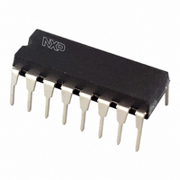
PCF8574AP,112 NXP Semiconductors, PCF8574AP,112 Datasheet - Page 7

PCF8574AP,112
Manufacturer Part Number
PCF8574AP,112
Description
IC I/O EXPANDER I2C 8B 16DIP
Manufacturer
NXP Semiconductors
Datasheet
1.PCF8574ATS3118.pdf
(24 pages)
Specifications of PCF8574AP,112
Package / Case
16-DIP (0.300", 7.62mm)
Interface
I²C
Number Of I /o
8
Interrupt Output
Yes
Frequency - Clock
100KHz
Voltage - Supply
2.5 V ~ 6 V
Operating Temperature
-40°C ~ 85°C
Mounting Type
Through Hole
Includes
POR
Logic Family
PCF8574
Number Of Lines (input / Output)
8.0 / 8.0
Operating Supply Voltage
2.5 V to 6 V
Power Dissipation
400 mW
Operating Temperature Range
- 40 C to + 85 C
Logic Type
I/O Expander
Maximum Clock Frequency
100 KHz
Mounting Style
Through Hole
Number Of Input Lines
8.0
Number Of Output Lines
8.0
Output Current
25 mA
Lead Free Status / RoHS Status
Lead free / RoHS Compliant
For Use With
568-3615 - DEMO BOARD I2C
Lead Free Status / Rohs Status
Lead free / RoHS Compliant
Other names
568-1073-5
933851670112
PCF8574APN
933851670112
PCF8574APN
Available stocks
Company
Part Number
Manufacturer
Quantity
Price
Company:
Part Number:
PCF8574AP,112
Manufacturer:
TI
Quantity:
7 820
Philips Semiconductors
6
The I
different ICs or modules. The two lines are a serial data
line (SDA) and a serial clock line (SCL). Both lines must be
connected to a positive supply via a pull-up resistor when
connected to the output stages of a device. Data transfer
may be initiated only when the bus is not busy.
6.1
One data bit is transferred during each clock pulse. The
data on the SDA line must remain stable during the HIGH
period of the clock pulse as changes in the data line at this
time will be interpreted as control signals (see Fig.5).
2002 Nov 22
handbook, full pagewidth
handbook, full pagewidth
Remote 8-bit I/O expander for I
CHARACTERISTICS OF THE I
2
C-bus is for 2-way, 2-line communication between
Bit transfer
SDA
SCL
TRANSMITTER /
SDA
SCL
RECEIVER
MASTER
START condition
SDA
SCL
S
2
C-BUS
Fig.6 Definition of start and stop conditions.
RECEIVER
SLAVE
Fig.7 System configuration.
data valid
data line
stable;
2
C-bus
Fig.5 Bit transfer.
TRANSMITTER /
RECEIVER
SLAVE
7
allowed
change
of data
6.2
Both data and clock lines remain HIGH when the bus is not
busy. A HIGH-to-LOW transition of the data line, while the
clock is HIGH is defined as the start condition (S).
A LOW-to-HIGH transition of the data line while the clock
is HIGH is defined as the stop condition (P) (see Fig.6).
6.3
A device generating a message is a ‘transmitter’, a device
receiving is the ‘receiver’. The device that controls the
message is the ‘master’ and the devices which are
controlled by the master are the ‘slaves’ (see Fig.7).
Start and stop conditions
System configuration
TRANSMITTER
MASTER
STOP condition
MBC621
P
MBC622
TRANSMITTER /
RECEIVER
SDA
MASTER
SCL
Product specification
PCF8574
MBA605


