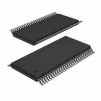
PCA9506DGG,518 NXP Semiconductors, PCA9506DGG,518 Datasheet - Page 18

PCA9506DGG,518
Manufacturer Part Number
PCA9506DGG,518
Description
IC I/O EXPANDER I2C 40B 56TSSOP
Manufacturer
NXP Semiconductors
Specifications of PCA9506DGG,518
Package / Case
56-TSSOP
Interface
I²C
Number Of I /o
40
Interrupt Output
Yes
Frequency - Clock
400kHz
Voltage - Supply
2.3 V ~ 5.5 V
Operating Temperature
-40°C ~ 85°C
Mounting Type
Surface Mount
Includes
POR
Logic Family
PCA9506
Number Of Lines (input / Output)
40.0 / 40.0
Operating Supply Voltage
2.3 V to 5.5 V
Power Dissipation
500 mW
Operating Temperature Range
- 40 C to + 85 C
Input Voltage
5.5 V
Logic Type
I/O Expander
Maximum Clock Frequency
400 KHz
Mounting Style
SMD/SMT
Number Of Input Lines
40.0
Number Of Output Lines
40.0
Output Current
50 mA
Output Voltage
5.5 V
Operating Temperature (min)
-40C
Operating Temperature Classification
Industrial
Operating Temperature (max)
85C
Package Type
TSSOP
Rad Hardened
No
Lead Free Status / RoHS Status
Lead free / RoHS Compliant
Lead Free Status / RoHS Status
Lead free / RoHS Compliant, Lead free / RoHS Compliant
Other names
935280798518
PCA9506DGG-T
PCA9506DGG-T
PCA9506DGG-T
PCA9506DGG-T
Fig 14. Read from Input Port, Output Port, I/O Configuration, Polarity Inversion or Mask Interrupt registers
If AI = 0, the same register is read during the whole sequence.
If AI = 1, the register value is incremented after each read. When the last register bank is read, it rolls over to the first byte of the category (see category definition in
Section 7.2 “Command
The INT signal is released only when the last register containing an input that changed has been read. For example, when IO2_4 and IO4_7 change at the same time and
an Input Port register’s read sequence is initiated, starting with IP0, INT is released after IP4 is read (and not after IP2 is read).
SDA
S
START condition
0 1 0 0
register determined by D[5:0]
slave address
data from register
first byte
DATA
register”).
A2 A1 A0
acknowledge
from slave
R/W
0
A
A
acknowledge from master
1 0 D5 D4 D3 D2 D1 D0
AI = 1
command register
data from register
second byte
DATA
D[5:0] = 00 0000 for Input Port register bank 0
D[5:0] = 00 1000 for Output Port register bank 0
D[5:0] = 01 0000 for Polarity Inversion register bank 0
D[5:0] = 01 1000 for Configuration register bank 0
D[5:0] = 10 0000 for Mask Interrupt register bank 0
A
acknowledge from slave
acknowledge from master
A
Sr
repeated START condition
0 1 0 0
slave address
A2 A1 A0
R/W
1
data from register
A
acknowledge from slave
At this moment master-transmitter becomes master-receiver,
and slave-receiver becomes slave-transmitter.
last byte
DATA
(cont.)
no acknowledge from master
A
P
STOP
condition
002aab499


