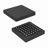
SCAN921226SLC/NOPB National Semiconductor, SCAN921226SLC/NOPB Datasheet

SCAN921226SLC/NOPB
Specifications of SCAN921226SLC/NOPB
*SCAN921226SLC/NOPB
SCAN921226SLC
Available stocks
Related parts for SCAN921226SLC/NOPB
SCAN921226SLC/NOPB Summary of contents
Page 1
... Deserializer to use the synchronization-to-random-data feature. By using Block Diagrams © 2004 National Semiconductor Corporation the synchronization mode, the Deserializer will establish lock to a signal within specified lock times. In addition, the em- bedded clock guarantees a transition on the bus every 12-bit cycle ...
Page 2
Block Diagrams (Continued) Functional Description The SCAN921025 and SCAN921226 are a 10-bit Serializer and Deserializer chipset designed to transmit data over dif- ferential backplanes at clock speeds from MHz. The chipset is also capable of driving data ...
Page 3
Data Transfer (Continued) high, PWRDN = high, and SYNC1 and SYNC2 are low. When DEN is driven low, the Serializer output pins will enter TRI-STATE. When the Deserializer synchronizes to the Serializer, the LOCK pin is low. The Deserializer locks ...
Page 4
Test Modes (Continued) system clocks (At a SCLK of 66Mhz and TCK of 1MHz this allows for 66 TCK cycles). This is not a concern when both devices are on the same scan chain or LSP, however, it can be ...
Page 5
Absolute Maximum Ratings Supply Voltage ( LVCMOS/LVTTL Input Voltage −0. LVCMOS/LVTTL Output Voltage −0. Bus LVDS Receiver Input Voltage Bus LVDS Driver Output Voltage Bus LVDS Output Short Circuit Duration Junction Temperature Storage Temperature ...
Page 6
Electrical Characteristics Over recommended operating supply and temperature ranges unless otherwise specified. Symbol Parameter DESERIALIZER Bus LVDS DC SPECIFICATIONS (apply to pins RI+ and RI−) VTH Differential Threshold High Voltage VTL Differential Threshold Low Voltage I Input Current IN SERIALIZER ...
Page 7
Serializer Switching Characteristics Over recommended operating supply and temperature ranges unless otherwise specified. Symbol Parameter t DIN (0-9) Setup to TCLK DIS t DIN (0-9) Hold from TCLK DIH ± HIGH to HZD TRI-STATE Delay ± ...
Page 8
Deserializer Switching Characteristics Over recommended operating supply and temperature ranges unless otherwise specified. Symbol Parameter t RCLK Duty Cycle RDC t HIGH to TRI-STATE Figure 14 HZR Delay t LOW to TRI-STATE LZR Delay t TRI-STATE to HIGH ZHR Delay ...
Page 9
AC Timing Diagrams and Test Circuits FIGURE 2. “Worst Case” Serializer ICC Test Pattern FIGURE 3. “Worst Case” Deserializer ICC Test Pattern FIGURE 4. Serializer Bus LVDS Output Load and Transition Times FIGURE 5. Deserializer CMOS/TTL Output Load and Transition ...
Page 10
AC Timing Diagrams and Test Circuits Timing shown for TCLK_R/F = LOW FIGURE 8. Serializer TRI-STATE Test Circuit and Timing www.national.com (Continued) FIGURE 6. Serializer Input Clock Transition Time FIGURE 7. Serializer Setup/Hold Times 10 20024807 20024808 20024809 ...
Page 11
AC Timing Diagrams and Test Circuits FIGURE 9. Serializer PLL Lock Time, and PWRDN TRI-STATE Delays (Continued) FIGURE 10. SYNC Timing Delays FIGURE 11. Serializer Delay 11 20024810 20024823 20024811 www.national.com ...
Page 12
AC Timing Diagrams and Test Circuits Timing shown for RCLK_R/F = LOW Duty Cycle ( RDC FIGURE 14. Deserializer TRI-STATE Test Circuit and Timing www.national.com (Continued) FIGURE 12. Deserializer Delay FIGURE 13. Deserializer Data Valid Out Times 12 ...
Page 13
AC Timing Diagrams and Test Circuits FIGURE 15. Deserializer PLL Lock Times and PWRDN TRI-STATE Delays FIGURE 16. Deserializer PLL Lock Time from SyncPAT (Continued) 13 20024815 20024822 www.national.com ...
Page 14
AC Timing Diagrams and Test Circuits + − (DO )–( Differential output signal is shown as (DO+)–(DO−), device in Data Transfer mode. www.national.com (Continued) 20024816 FIGURE 17. V Diagram OD 14 ...
Page 15
Application Information USING THE SCAN921025 AND SCAN921226 The Serializer and Deserializer chipset is an easy to use transmitter and receiver pair that sends 10 bits of parallel LVTTL data over a serial Bus LVDS link up to 800 Mbps. An ...
Page 16
Application Information USING T AND T TO VALIDATE SIGNAL DJIT RNM QUALITY The parameter t is calculated by first measuring how RNM much of the ideal bit the receiver needs to ensure correct sampling. After determining this amount, what remains ...
Page 17
Application Information t is the ideal noise margin on the left of the figure negative value to indicate early with respect to ideal. RNMI the ideal noise margin on the right of the above figure, ...
Page 18
Pin Diagrams www.national.com SCAN921025SLC - Serializer (Top View) 20024830 SCAN921226SLC - Deserializer (Top View) 20024831 18 ...
Page 19
Serializer Pin Description Pin Name I/O DIN I TCLKR/F I DO+ O DO− O DEN I PWRDN I TCLK I SYNC I DVCC I DGND I AVCC I AGND I TDI I TDO O TMS I TCK I TRST I ...
Page 20
Deserializer Pin Description Pin Name I/O ROUT O RCLKR/F I RI+ I RI− I PWRDN I LOCK O RCLK O REN I DVCC I DGND I AVCC I AGND I REFCLK I TDI I TDO O TMS I TCK I ...
Page 21
... BANNED SUBSTANCE COMPLIANCE National Semiconductor certifies that the products and packing materials meet the provisions of the Customer Products Stewardship Specification (CSP-9-111C2) and the Banned Substances and Materials of Interest Specification (CSP-9-111S2) and contain no ‘‘Banned Substances’’ as defined in CSP-9-111S2. ...


