SCAN921226SLC/NOPB National Semiconductor, SCAN921226SLC/NOPB Datasheet - Page 15
SCAN921226SLC/NOPB
Manufacturer Part Number
SCAN921226SLC/NOPB
Description
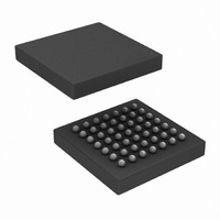
IC DESERIALIZER 10BIT 49FBGA
Manufacturer
National Semiconductor
Series
SCANr
Datasheet
1.SCAN921226SLCNOPB.pdf
(21 pages)
Specifications of SCAN921226SLC/NOPB
Function
Deserializer
Data Rate
800Mbps
Input Type
LVDS
Output Type
LVDS
Number Of Inputs
1
Number Of Outputs
10
Voltage - Supply
3 V ~ 3.6 V
Operating Temperature
-40°C ~ 125°C
Mounting Type
Surface Mount
Package / Case
49-FBGA
Lead Free Status / RoHS Status
Lead free / RoHS Compliant
Other names
*SCAN921226SLC
*SCAN921226SLC/NOPB
SCAN921226SLC
*SCAN921226SLC/NOPB
SCAN921226SLC
Available stocks
Company
Part Number
Manufacturer
Quantity
Price
Company:

Part Number:
SCAN921226SLC/NOPB
Manufacturer:
Texas Instruments
Quantity:
10 000


Application Information
USING THE SCAN921025 AND SCAN921226
The Serializer and Deserializer chipset is an easy to use
transmitter and receiver pair that sends 10 bits of parallel
LVTTL data over a serial Bus LVDS link up to 800 Mbps. An
on-board PLL serializes the input data and embeds two clock
bits within the data stream. The Deserializer uses a separate
reference clock (REFCLK) and an onboard PLL to extract
the clock information from the incoming data stream and
then deserialize the data. The Deserializer monitors the
incoming clock information, determines lock status, and as-
serts the LOCK output high when loss of lock occurs.
POWER CONSIDERATIONS
An all CMOS design of the Serializer and Deserializer makes
them inherently low power devices. In addition, the constant
current source nature of the Bus LVDS outputs minimizes
the slope of the speed vs. I
designs.
POWERING UP THE DESERIALIZER
The SCAN921226 can be powered up at any time by follow-
ing the proper sequence. The REFCLK input can be running
before the Deserializer powers up, and it must be running in
order for the Deserializer to lock to incoming data. The
Deserializer outputs will remain in TRI-STATE until the De-
serializer detects data transmission at its inputs and locks to
the incoming data stream.
TRANSMITTING DATA
Once you power up the Serializer and Deserializer, they
must be phase locked to each other to transmit data. Phase
locking occurs when the Deserializer locks to incoming data
or when the Serializer sends patterns. The Serializer sends
SYNC patterns whenever the SYNC1 or SYNC2 inputs are
high. The LOCK output of the Deserializer remains high until
it has locked to the incoming data stream. Connecting the
LOCK output of the Deserializer to one of the SYNC inputs of
the Serializer will guarantee that enough SYNC patterns are
sent to achieve Deserializer lock.
The Deserializer can also lock to incoming data by simply
powering up the device and allowing the “random lock”
circuitry to find and lock to the data stream.
While the Deserializer LOCK output is low, data at the De-
serializer outputs (ROUT0-9) is valid, except for the specific
case of loss of lock during transmission which is further
discussed in the "Recovering from LOCK Loss" section be-
low.
NOISE MARGIN
The Deserializer noise margin is the amount of input jitter
(phase noise) that the Deserializer can tolerate and still
reliably receive data. Various environmental and systematic
factors include:
out-of-band noise)
RECOVERING FROM LOCK LOSS
In the case where the Deserializer loses lock during data
transmission, up to 3 cycles of data that were previously
received can be invalid. This is due to the delay in the lock
detection circuit. The lock detect circuit requires that invalid
Serializer: TCLK jitter, V
Media: ISI, Large V
Deserializer: V
CC
noise
CM
shifts
CC
CC
curve of conventional CMOS
noise (noise bandwidth and
15
clock information be received 4 times in a row to indicate
loss of lock. Since clock information has been lost, it is
possible that data was also lost during these cycles. There-
fore, after the Deserializer relocks to the incoming data
stream and the Deserializer LOCK pin goes low, at least
three previous data cycles should be suspect for bit errors.
The Deserializer can relock to the incoming data stream by
making the Serializer resend SYNC patterns, as described
above, or by random locking, which can take more time,
depending on the data patterns being received.
HOT INSERTION
All the BLVDS devices are hot pluggable if you follow a few
rules. When inserting, ensure the Ground pin(s) makes con-
tact first, then the VCC pin(s), and then the I/O pins. When
removing, the I/O pins should be unplugged first, then the
VCC, then the Ground. Random lock hot insertion is illus-
trated inFigure 21 .
PCB CONSIDERATIONS
The Bus LVDS Serializer and Deserializer should be placed
as close to the edge connector as possible. In multiple
Deserializer applications, the distance from the Deserializer
to the slot connector appears as a stub to the Serializer
driving the backplane traces. Longer stubs lower the imped-
ance of the bus, increase the load on the Serializer, and
lower the threshold margin at the Deserializers. Deserializer
devices should be placed much less than one inch from slot
connectors. Because transition times are very fast on the
Serializer Bus LVDS outputs, reducing stub lengths as much
as possible is the best method to ensure signal integrity.
TRANSMISSION MEDIA
The Serializer and Deserializer can also be used in point-to-
point configuration of a backplane, through a PCB trace, or
through twisted pair cable. In point-to-point configuration, the
transmission media need only be terminated at the receiver
end. Please note that in point-to-point configuration, the
potential of offsetting the ground levels of the Serializer vs.
the Deserializer must be considered. Also, Bus LVDS pro-
vides a +/− 1.2V common mode range at the receiver inputs.
FAILSAFE BIASING FOR THE SCAN921226
The SCAN921226 has an improved input threshold sensitiv-
ity of +/− 50mV versus +/− 100mV for the DS92LV1210 or
DS92LV1212. This allows for greater differential noise mar-
gin in the SCAN921226. However, in cases where the re-
ceiver input is not being actively driven, the increased sen-
sitivity of the SCAN921226 can pickup noise as a signal and
cause unintentional locking. For example, this can occur
when the input cable is disconnected.
External resistors can be added to the receiver circuit board
to prevent noise pick-up. Typically, the non-inverting receiver
input is pulled up and the inverting receiver input is pulled
down by high value resistors. the pull-up and pull-down
resistors (R
termination resistor (R
when they are not connected to an active driver. The value of
the pull-up and pull-down resistors should be chosen so that
enough current is drawn to provide a +15mV drop across the
termination resistor. Please see Figure 18for the Failsafe
Biasing Setup.
1
and R
2
) provide a current path through the
L
) which biases the receiver inputs
www.national.com
Related parts for SCAN921226SLC/NOPB
Image
Part Number
Description
Manufacturer
Datasheet
Request
R

Part Number:
Description:
30-80 MHz 10 Bit Bus LVDS Serializer and Deserializer with IEEE 1149.1 (JTAG) and at-speed BIST
Manufacturer:
NSC [National Semiconductor]
Datasheet:

Part Number:
Description:
National Semiconductor [8-Bit D/A Converter]
Manufacturer:
National Semiconductor
Datasheet:
Part Number:
Description:
National Semiconductor [Media Coprocessor]
Manufacturer:
National Semiconductor
Datasheet:
Part Number:
Description:
Digitally Controlled Tone and Volume Circuit with Stereo Audio Power Amplifier, Microphone Preamp Stage and National 3D Sound
Manufacturer:
National Semiconductor
Datasheet:
Part Number:
Description:
Digitally Controlled Tone and Volume Circuit with Stereo Audio Power Amplifier, Microphone Preamp Stage and National 3D Sound
Manufacturer:
National Semiconductor
Datasheet:
Part Number:
Description:
AC97 Rev 2 Codec with Sample Rate Conversion and National 3D Sound
Manufacturer:
National Semiconductor
Part Number:
Description:
Manufacturer:
National Semiconductor
Datasheet:
Part Number:
Description:
Manufacturer:
National Semiconductor
Datasheet:
Part Number:
Description:
General Purpose, Low Voltage, Low Power, Rail-to-Rail Output Operational Amplifiers
Manufacturer:
National Semiconductor
Datasheet:
Part Number:
Description:
8-bit 20 MSPS flash A/D converter.
Manufacturer:
National Semiconductor
Datasheet:
Part Number:
Description:
Low Noise Quad Operational Amplifier
Manufacturer:
National Semiconductor
Datasheet:
Part Number:
Description:
Quad Differential Line Receivers
Manufacturer:
National Semiconductor
Datasheet:
Part Number:
Description:
Quad High Speed Trapezoidal? Bus Transceiver
Manufacturer:
National Semiconductor
Datasheet:
Part Number:
Description:
Dual Line Receiver
Manufacturer:
National Semiconductor
Datasheet: