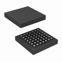
SCAN921226SLC/NOPB National Semiconductor, SCAN921226SLC/NOPB Datasheet - Page 8

SCAN921226SLC/NOPB
Manufacturer Part Number
SCAN921226SLC/NOPB
Description
IC DESERIALIZER 10BIT 49FBGA
Manufacturer
National Semiconductor
Series
SCANr
Datasheet
1.SCAN921226SLCNOPB.pdf
(21 pages)
Specifications of SCAN921226SLC/NOPB
Function
Deserializer
Data Rate
800Mbps
Input Type
LVDS
Output Type
LVDS
Number Of Inputs
1
Number Of Outputs
10
Voltage - Supply
3 V ~ 3.6 V
Operating Temperature
-40°C ~ 125°C
Mounting Type
Surface Mount
Package / Case
49-FBGA
Lead Free Status / RoHS Status
Lead free / RoHS Compliant
Other names
*SCAN921226SLC
*SCAN921226SLC/NOPB
SCAN921226SLC
*SCAN921226SLC/NOPB
SCAN921226SLC
Available stocks
Company
Part Number
Manufacturer
Quantity
Price
Company:
Part Number:
SCAN921226SLC/NOPB
Manufacturer:
Texas Instruments
Quantity:
10 000
www.national.com
Symbol
t
t
t
t
t
t
t
t
t
t
f
t
t
t
t
t
t
t
RDC
HZR
LZR
ZHR
ZLR
DSR1
DSR2
ZHLK
RNMI-R
RNMI-L
MAX
S
H
S
H
W
W
REC
Symbol
Deserializer Switching Characteristics
Over recommended operating supply and temperature ranges unless otherwise specified.
SCAN Circuitry Timing Requirements
Note 1: “Absolute Maximum Ratings” are those values beyond which the safety of the device cannot be guaranteed. They are not meant to imply that the devices
should be operated at these limits. The table of “Electrical Characteristics” specifies conditions of device operation.
Note 2: Typical values are given for V
Note 3: Current into device pins is defined as positive. Current out of device pins is defined as negative. Voltages are referenced to ground except VOD, ∆VOD,
VTH and VTL which are differential voltages.
Note 4: t
Note 5: Because the Serializer is in TRI-STATE mode, the Deserializer will lose PLL lock and have to resynchronize before data transfer.
Note 6: t
Note 7: For the purpose of specifying deserializer PLL performance, tDSR1 and tDSR2 are specified with the REFCLK running and stable, and with specific
conditions for the incoming data stream (SYNCPATs). It is recommended that the derserializer be initialized using either t
time required for the deserializer to indicate lock upon power-up or when leaving the power-down mode. Synchronization patterns should be sent to the device before
initiating either condition. t
not receiving data to receiving synchronization patterns (SYNCPATs).
Note 8: t
Margin is Guaranteed By Design (GBD) using statistical analysis.
RCLK Duty Cycle
HIGH to TRI-STATE
Delay
LOW to TRI-STATE
Delay
TRI-STATE to HIGH
Delay
TRI-STATE to LOW
Delay
Deserializer PLL Lock
Time from PWRDWN
(with SYNCPAT)
Deserializer PLL Lock
time from SYNCPAT
TRI-STATE to HIGH
Delay (power-up)
Ideal Noise Margin Right Figure 20
Ideal Noise Margin Left
LLHT
DJIT
RNM
Maximum TCK Clock
Frequency
TDI to TCK, H or L
TDI to TCK, H or L
TMS to TCK, H or L
TMS to TCK, H or L
TCK Pulse Width, H or L
TRST Pulse Width, L
Recovery Time, TRST to
TCK
specifications are Guaranteed By Design using statistical analysis.
is a measure of how much phase noise (jitter) the deserializer can tolerate in the incoming data stream before bit errors occur. The Deserializer Noise
and t
Parameter
LHLT
Parameter
specifications are Guaranteed By Design (GBD) using statistical analysis.
DSR2
is the time required to indicate lock for the powered-up and enabled deserializer when the input (RI+ and RI-) conditions change from
CC
Figure 14
Figure 15
Figure 16
(Note 7)
Figure 20
= 3.3V and T
Conditions
R
L
= 500Ω, C
A
Conditions
= +25˚C.
L
Pin/Freq.
Rout(0-9)
= 35 pF
30MHz
80MHz
30MHz
80MHz
LOCK
MHz
MHz
80
80
8
(Continued)
25.0
10.0
Min
-385
1.0
2.0
2.5
1.5
2.5
2.0
Min
45
50.0
Typ
0.65
0.29
Typ
2.8
2.8
4.2
4.2
1.7
1.0
3.7
50
DSR1
timing or t
DSR2
Max
+350
Max
3.5
2.5
1.5
0.8
55
10
10
10
10
12
timing. t
DSR1
Units
MHz
is the
Units
ns
ns
ns
ns
ns
ns
ns
ns
ns
ns
ns
µs
µs
µs
µs
ns
ps
ps
%


