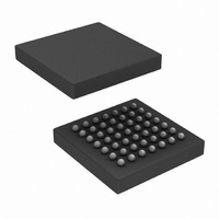
SCAN921226SLC/NOPB National Semiconductor, SCAN921226SLC/NOPB Datasheet - Page 19

SCAN921226SLC/NOPB
Manufacturer Part Number
SCAN921226SLC/NOPB
Description
IC DESERIALIZER 10BIT 49FBGA
Manufacturer
National Semiconductor
Series
SCANr
Datasheet
1.SCAN921226SLCNOPB.pdf
(21 pages)
Specifications of SCAN921226SLC/NOPB
Function
Deserializer
Data Rate
800Mbps
Input Type
LVDS
Output Type
LVDS
Number Of Inputs
1
Number Of Outputs
10
Voltage - Supply
3 V ~ 3.6 V
Operating Temperature
-40°C ~ 125°C
Mounting Type
Surface Mount
Package / Case
49-FBGA
Lead Free Status / RoHS Status
Lead free / RoHS Compliant
Other names
*SCAN921226SLC
*SCAN921226SLC/NOPB
SCAN921226SLC
*SCAN921226SLC/NOPB
SCAN921226SLC
Available stocks
Company
Part Number
Manufacturer
Quantity
Price
Company:
Part Number:
SCAN921226SLC/NOPB
Manufacturer:
Texas Instruments
Quantity:
10 000
DIN
TCLKR/F
DO+
DO−
DEN
PWRDN
TCLK
SYNC
DVCC
DGND
AVCC
AGND
TDI
TDO
TMS
TCK
TRST
N/C
Serializer Pin Description
Pin Name
N/A
I/O
O
O
O
I
I
I
I
I
I
I
I
I
I
I
I
I
I
E1, E2, F2, F4
D1, D2, D3,
A3, B1, C1,
A1, C2, F5,
A5, A6, B4,
B5, B6, C6,
A2, A7, B2,
C5, D4, F6,
C3, C4, E5
Ball Id.
E6, G4
B7, G5
G6, G7
A4, B3
E7, F7
G3
D7
D5
D6
C7
G1
G2
E4
F1
E3
F3
Data Input. LVTTL levels inputs. Data on these pins are loaded into
a 10-bit input register.
Transmit Clock Rising/Falling strobe select. LVTTL level input.
Selects TCLK active edge for strobing of DIN data. High selects
rising edge. Low selects falling edge.
+ Serial Data Output. Non-inverting Bus LVDS differential output.
− Serial Data Output. Inverting Bus LVDS differential output.
Serial Data Output Enable. LVTTL level input. A low puts the Bus
LVDS outputs in TRI-STATE.
Powerdown. LVTTL level input. PWRDN driven low shuts down the
PLL and TRI-STATEs outputs putting the device into a low power
sleep mode.
Transmit Clock. LVTTL level input. Input for 30MHz – 80MHz
system clock.
Assertion of SYNC (high) for at least 1024 synchronization symbols
to be transmitted on the Bus LVDS serial output. Synchronization
symbols continue to be sent if SYNC continues to be asserted. TTL
level input. The two SYNC pins are ORed.
Digital Circuit power supply.
Digital Circuit ground.
Analog power supply (PLL and Analog Circuits).
Analog ground (PLL and Analog Circuits).
Test Data Input to support IEEE 1149.1. There is an internal pullup
resistor that defaults this input to high per IEEE 1149.1.
Test Data Output to support IEEE 1149.1
Test Mode Select Input to support IEEE 1149.1. There is an
internal pullup resistor that defaults this input to high per IEEE
1149.1.
Test Clock Input to support IEEE 1149.1
Test Reset Input to support IEEE 1149.1. There is an internal
pullup resistor that defaults this input to high per IEEE 1149.1.
Leave open circuit, do not connect
19
Description
www.national.com


