SCAN921226SLC/NOPB National Semiconductor, SCAN921226SLC/NOPB Datasheet - Page 6
SCAN921226SLC/NOPB
Manufacturer Part Number
SCAN921226SLC/NOPB
Description
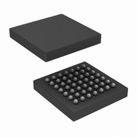
IC DESERIALIZER 10BIT 49FBGA
Manufacturer
National Semiconductor
Series
SCANr
Datasheet
1.SCAN921226SLCNOPB.pdf
(21 pages)
Specifications of SCAN921226SLC/NOPB
Function
Deserializer
Data Rate
800Mbps
Input Type
LVDS
Output Type
LVDS
Number Of Inputs
1
Number Of Outputs
10
Voltage - Supply
3 V ~ 3.6 V
Operating Temperature
-40°C ~ 125°C
Mounting Type
Surface Mount
Package / Case
49-FBGA
Lead Free Status / RoHS Status
Lead free / RoHS Compliant
Other names
*SCAN921226SLC
*SCAN921226SLC/NOPB
SCAN921226SLC
*SCAN921226SLC/NOPB
SCAN921226SLC
Available stocks
Company
Part Number
Manufacturer
Quantity
Price
Company:

Part Number:
SCAN921226SLC/NOPB
Manufacturer:
Texas Instruments
Quantity:
10 000


www.national.com
DESERIALIZER Bus LVDS DC SPECIFICATIONS (apply to pins RI+ and RI−)
VTH
VTL
I
SERIALIZER SUPPLY CURRENT (apply to pins DVCC and AVCC)
I
I
DESERIALIZER SUPPLY CURRENT (apply to pins DVCC and AVCC)
I
I
SCAN CIRCUITRY DC SPECIFICATIONS, SERIALIZER AND DESERIALIZER (applies to SCAN pins as noted)
V
V
V
I
I
I
V
V
I
I
t
t
t
t
t
t
t
Symbol
IN
CCD
CCXD
CCR
CCXR
IH
IL
ILR
OS
OZ
TCP
TCIH
TCIL
CLKT
JIT
LLHT
LHLT
IH
IL
CL
OH
OL
Symbol
Electrical Characteristics
Over recommended operating supply and temperature ranges unless otherwise specified.
Serializer Timing Requirements for TCLK
Over recommended operating supply and temperature ranges unless otherwise specified.
Serializer Switching Characteristics
Over recommended operating supply and temperature ranges unless otherwise specified.
Symbol
Bus LVDS Low-to-High
Transition Time
Bus LVDS High-to-Low
Transition Time
Transmit Clock Period
Transmit Clock High Time
Transmit Clock Low Time
TCLK Input Transition
Time
TCLK Input Jitter
Differential Threshold High Voltage
Differential Threshold Low Voltage
Input Current
Serializer Supply Current
Worst Case
Serializer Supply Current Powerdown PWRDN = 0.8V, f = 80MHz
Deserializer Supply Current
Worst Case
Deserializer Supply Current
Powerdown
High Level Input Voltage
Low Level Input Voltage
Input Clamp Voltage
Input Current
Input Current
Input Current
High Level Output Voltage
Low Level Output Voltage
Output Short Circuit Current
TRI-STATE Output Current
Parameter
Parameter
Parameter
R
C
Figure 4
(Note 4)
L
L
=10pF to GND
= 27Ω
Conditions
Conditions
(Continued)
VCM = +1.1V
V
V
RL = 27Ω
Figure 2
C
Figure 3
PWRDN = 0.8V, REN = 0.8V
V
and TRST
V
and TRST
V
TDI, and TRST
V
TDI, and TRST
V
V
TRST
V
V
V
PWRDN or REN = 0.8V, V
IN
IN
CC
CC
CC
CC
CC
CC
CC
CC
CC
L
= 15 pF
= +2.4V, V
= 0V, V
= 3.0 to 3.6V, pins TCK, TMS, TDI,
= 3.0 to 3.6V, pins TCK, TMS, TDI,
= 3.0V, I
= 3.6V, V
= 3.6V, V
= 3.6V, V
= 3.0V, I
= 3.0V, I
= 3.6V, V
CC
6
CL
OH
OL
IN
IN
IN
OUT
CC
= 3.6V or 0V
= −18 mA, pins TCK, TMS,
Conditions
= 12 mA, TDO output
= 3.6V, pins TCK, TMS,
= 0.0V, TCK Input
= 0V, pins TMS, TDI, and
= −12 mA, TDO output
= 3.6V or 0V
0.4T
0.4T
= 0.0V, TDO output
12.5
Min
Min
OUT
f = 30 MHz
f = 80 MHz
f = 30 MHz
f = 80 MHz
= 0V or VCC
0.5T
0.5T
0.25
Typ
Typ
0.2
T
3
GND
Min
−50
−10
−10
−10
-10
-20
-15
2.0
2.2
±
−0.85
0.36
Typ
−12
100
0.2
-10
2.6
0.3
-90
Max
+6
±
0.05
45
90
50
-1
0.4
0.4
1
0
0.6T
0.6T
Max
33.3
150
1
6
Max
−1.5
-120
V
+50
+10
+10
105
120
+10
+10
1.0
1.0
0.8
0.5
60
75
CC
Units
(RMS)
Units
Units
ns
ns
mV
mV
mA
mA
mA
mA
mA
mA
mA
ns
ns
ns
ns
ps
µA
µA
µA
µA
µA
µA
V
V
V
V
V
Related parts for SCAN921226SLC/NOPB
Image
Part Number
Description
Manufacturer
Datasheet
Request
R

Part Number:
Description:
30-80 MHz 10 Bit Bus LVDS Serializer and Deserializer with IEEE 1149.1 (JTAG) and at-speed BIST
Manufacturer:
NSC [National Semiconductor]
Datasheet:

Part Number:
Description:
National Semiconductor [8-Bit D/A Converter]
Manufacturer:
National Semiconductor
Datasheet:
Part Number:
Description:
National Semiconductor [Media Coprocessor]
Manufacturer:
National Semiconductor
Datasheet:
Part Number:
Description:
Digitally Controlled Tone and Volume Circuit with Stereo Audio Power Amplifier, Microphone Preamp Stage and National 3D Sound
Manufacturer:
National Semiconductor
Datasheet:
Part Number:
Description:
Digitally Controlled Tone and Volume Circuit with Stereo Audio Power Amplifier, Microphone Preamp Stage and National 3D Sound
Manufacturer:
National Semiconductor
Datasheet:
Part Number:
Description:
AC97 Rev 2 Codec with Sample Rate Conversion and National 3D Sound
Manufacturer:
National Semiconductor
Part Number:
Description:
Manufacturer:
National Semiconductor
Datasheet:
Part Number:
Description:
Manufacturer:
National Semiconductor
Datasheet:
Part Number:
Description:
General Purpose, Low Voltage, Low Power, Rail-to-Rail Output Operational Amplifiers
Manufacturer:
National Semiconductor
Datasheet:
Part Number:
Description:
8-bit 20 MSPS flash A/D converter.
Manufacturer:
National Semiconductor
Datasheet:
Part Number:
Description:
Low Noise Quad Operational Amplifier
Manufacturer:
National Semiconductor
Datasheet:
Part Number:
Description:
Quad Differential Line Receivers
Manufacturer:
National Semiconductor
Datasheet:
Part Number:
Description:
Quad High Speed Trapezoidal? Bus Transceiver
Manufacturer:
National Semiconductor
Datasheet:
Part Number:
Description:
Dual Line Receiver
Manufacturer:
National Semiconductor
Datasheet: