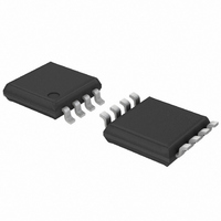
PCA9515ADP,118 NXP Semiconductors, PCA9515ADP,118 Datasheet - Page 16

PCA9515ADP,118
Manufacturer Part Number
PCA9515ADP,118
Description
IC I2C BUS REPEATER 8-TSSOP
Manufacturer
NXP Semiconductors
Type
Repeaterr
Datasheet
1.PCA9515ADP118.pdf
(18 pages)
Specifications of PCA9515ADP,118
Package / Case
8-TSSOP
Tx/rx Type
I²C Logic
Delay Time
113ns
Capacitance - Input
6pF
Voltage - Supply
2.3 V ~ 3.6 V
Current - Supply
800µA
Mounting Type
Surface Mount
Logic Family
PCA9515A
Operating Supply Voltage
2.3 V to 3.6 V
Power Dissipation
100 mW
Operating Temperature Range
- 40 C to + 85 C
Input Voltage
5.5 V
Logic Type
I2C Bus
Maximum Clock Frequency
400 KHz
Mounting Style
SMD/SMT
Output Current
50 mA
Output Voltage
5.5 V
Lead Free Status / RoHS Status
Lead free / RoHS Compliant
For Use With
OM6285 - EVAL BOARD I2C-2002-1A568-4002 - DEMO BOARD I2C
Lead Free Status / Rohs Status
Lead free / RoHS Compliant
Other names
568-1032-2
935275998118
PCA9515ADP-T
935275998118
PCA9515ADP-T
Available stocks
Company
Part Number
Manufacturer
Quantity
Price
Part Number:
PCA9515ADP,118
Manufacturer:
NXP/恩智浦
Quantity:
20 000
NXP Semiconductors
15. Revision history
Table 11.
PCA9515A_4
Product data sheet
Document ID
PCA9515A_4
Modifications:
PCA9515A_3
(9397 750 14098)
PCA9515A_2
(9397 750 13709)
PCA9515A_1
(9397 98 13237)
Revision history
Release date
20080411
20040929
20040709
20040617
•
•
•
•
•
•
•
•
The format of this data sheet has been redesigned to comply with the new identity guidelines of
NXP Semiconductors.
Legal texts have been adapted to the new company name where appropriate.
Section 1 “General
Table 2 “Pin
– appended “open-drain 5 V tolerant I/O” to the descriptions of SCL0 (pin 2), SDA0 (pin 3),
– appended “(internal pull-up with 100 k )” to the description of EN (pin 5)
Table 4 “Static characteristics (V
(V
– changed parameter description for I
– changed parameter description for I
– sub-section “Enable”: changed symbol/parameter from “I
Table 6 “Dynamic characteristics (V
(V
– changed symbol/parameter from “t
– changed symbol/parameter from “t
Added SMD package soldering information
Added
CC
CC
SDA1 (pin 6), and SCL1 (pin 7)
to “HIGH-level supply current” (moved “both channels HIGH” to Conditions column)
“LOW-level supply current” (moved “both channels LOW” to Conditions column)
LOW-level input current on pin EN”
added “EN HIGH before START condition” to Conditions column
added “EN HIGH after STOP condition” to Conditions column
= 2.3 V to 2.7
= 3.0 V to 3.6
Section 14 “Abbreviations”
description”:
Data sheet status
Product data sheet
Product data sheet
Product data sheet
Objective data sheet
description”, 4
V)”:
V)”:
Rev. 04 — 11 April 2008
CC
th
= 3.0 V to 3.6 V)”
CC
paragraph: 5
SET
HOLD
= 2.3 V to 2.7 V)”
CCL
CCH
, Enable to Start condition” to “t
from “quiescent supply current, both channels LOW” to
, Enable after Stop condition” to “t
from “quiescent supply current, both channels HIGH”
th
Change notice
-
-
-
-
and 6
and
th
and
Table 5 “Static characteristics
sentences re-written
IL
Table 7 “Dynamic characteristics
, input current LOW, EN” to “I
Supersedes
PCA9515A_3
PCA9515A_2
PCA9515A_1
-
su
PCA9515A
, set-up time”;
h
, hold time”;
© NXP B.V. 2008. All rights reserved.
I
2
C-bus repeater
IL(EN)
16 of 18
,


